Antminer S19 Hash Board Repair Manual
By THANOS MINING
April 23rd, 2022
It describes the troubleshooting of Bitmain Antminer S19 various faults, and explains how to use the test tools for accurate positioning.
New version of test fixture: Antminer S19 test fixture
I. Maintenance platform/tool/equipment preparation requirements
1. Platform requirements:
Rubber blanket repair workbench (workbench needs to be grounded), anti-static wristband and grounding.
2. Equipment requirements:
Constant temperature soldering iron (350℃ - 380℃) and pointed soldering iron tip are used for soldering small patches such as chip resistors and capacitors; heat gun, BGA rework station are used for chip/BGA disassembly and soldering; multimeter with soldering steel pin and heat-shrinkable T bush is used for easy measurement (Fluke is recommended); Oscilloscope (Agilent recommended), network cable (requirements: Internet connection, stable network)
3. Requirements for test tools:
APW12 power supply (APW12_12V-15V_V1.2 and power adapter cable (self made: use thick copper wires to connect the power supply at positive and negative poles and the hashboard. It is recommended to use 4AWG copper wires with a length of 60cm or less) for the hashboard. Use the test fixture of the V2.2010 control board. The positive and negative poles of the test fixture need to be installed with discharge resistors. It is recommended to use a cement resistor of 25 ohms and more than 100W.
4. Maintenance auxiliary materials/tool requirements:
Solder paste column M705, flux, board washing water with absolute alcohol; board washing water is used to clean up the solder residue after repair; thermal gel (specification: Fujipoly SPG-30B) is used to smear the surface of the chip after repair ;ball-planting steel mesh, solder absorption wire, solder ball (the ball diameter is recommended to be 0.4mm); when replacing a new chip, you need to tin the chip pins and then solder to the hashboard, and then lock large heat sinks after applying thermal gel evenly on the chip surface.
1) Barcode scanning gun (purchase reference link: https://item.jd.com/11829261868.html)
2) Port adapter board RS232/TTL adapter board 3.3V
(Purchase reference link: https://detail.tmall.com/item.htm?spm=a230r.1.14.6.751533f7AP9fR8&id=583960428696)
3) Self-made short-circuit probe (use pin wire for welding, require the heat-shrinkable T bush, prevent short circuit between probe and small heat sink)
5. Common maintenance spare material requirements:0402 resistance (0R, 51R, 10K, 4.7K,); 0402 capacitor (0.1uf, 1uf)
II. Maintenance requirements
1. Pay attention to the operation method when replacing the chip. After replacing any accessories, the PCB board shall have no obvious deformation. Check the replacement parts and the surrounding parts for open circuit and short circuit issues.
2. The maintenance operators must have certain electronic knowledge, more than one year of maintenance experience, and be proficient in BGA/QFN/LGA package soldering technology.
3. After repairing, the hashboard must be tested for more than two times to be OK before it can pass!
4. Check whether the tools and hashboard testers can work normally, determine the maintenance station to test software parameters, test fixture versions, etc.
5. In the test of repairing and replacing the chip, the chip needs to be tested first, and then the function test shall be performed after passing. The function test must ensure that the small heat sink is welded qualified. When installing the large heat sink, the surface of the chip must be evenly coated with thermal gel and the cooling fan shall be at full speed. When using the chassis to dissipate heat, 2 hashboards should be placed at the same time to form an air duct.
6. When measuring the signal, use 4 fans as assistance for heat dissipation, and the fans shall maintain full speed.
7. When powering on the hashboard, user must first connect the negative copper wire of the power supply, then the positive copper wire of the power supply, and finally plug in the signal cable. When removing, the order of installation must be reversed. First remove the signal cable, then remove the positive copper wire of the power supply, and finally remove the negative copper wire of the power supply. If the user do not follow this order, it is very easy to cause damage to R8, R9, U1, U2 (not all chips can be found). Before testing the pattern, the repaired hashboard must be cooled down before testing, otherwise it may cause PNG testing.
8. To replace a new chip, printing pins and soldering paste are required to ensure that the chip is pre-soldered and then soldered to the PCBA for repair
III. Hashboard tester making and matters needing attention
The supporting fixture of the hashboard tester should satisfy the heat dissipation of the hashboard and facilitate the measurement of signals
1. Use the 19 series hashboard tester SD card swiping program for the first time to update the hashboard tester control board FPGA, unzip it and copy it to the SD card, and then insert the card into the hashboard tester card slot; power on for about 1 minute and wait for the control board indicator to double flash 3 times, then the update is completed; (if it is not updated, it may cause a certain chip to be bad during the test)

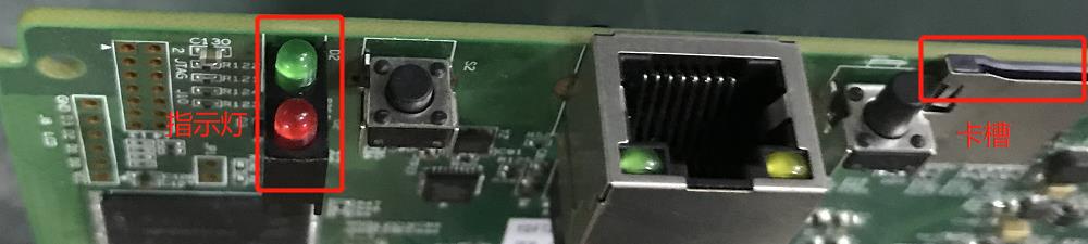
Figure 3-1
2. Make the test SD card according to the requirements, and directly unzip the compressed package of the single-sided heat sink inspection chip to make the SD card;
Figure 3-2
3. The test SD card will be made according to the requirements, and the double-sided heat sink 8-times Patter test needs to make an SD card, as shown in the figure below;

Figure 3-3
Figure 3-4
Figure 3-5
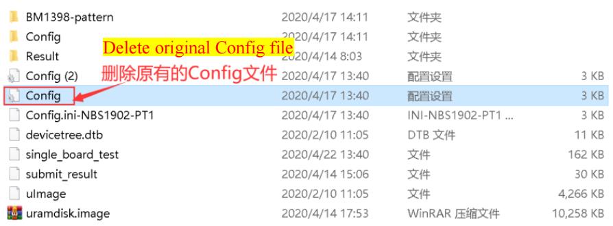
Figure 3-6
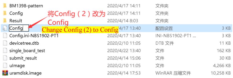
Figure 3-7
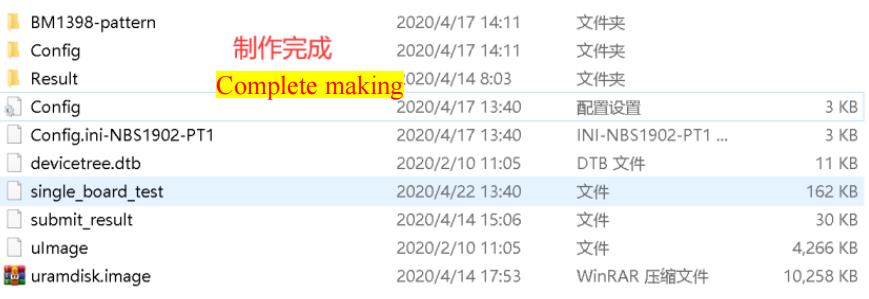
Figure 3-8
IV. Principle overview
1. Working structure of S19 hashboard:
The hashboard is composed of 76 BM1398 chips, which are divided into 38 groups (domains), and each group is composed of 2 ICs; the operating voltage of the BM1398 chip used in the S19 hashboard is 0.36V; for the 38th, 37th, 36th, 35th, 34th, 33rd, 32nd group (7 groups in total), LDO is powered by the 19V output from the boost circuit U9 and outputs 1.8V. The 30th group - the first group are supplied by VDD13.64V through the LDO to provide 1.8V, and the voltage of each domain retreated is reduced by 0.36V. All 0.8V is provided by the 1.8V output of this domain via LDO, as shown in Figure 4-1;

Figure 4-1
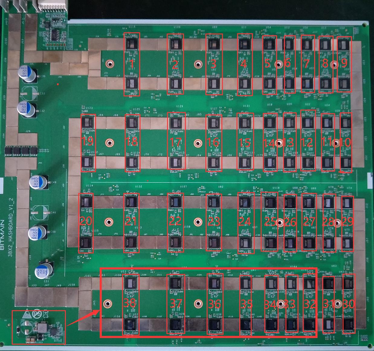
Figure 4-2
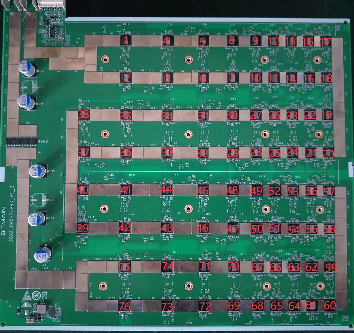
Figure 4-3
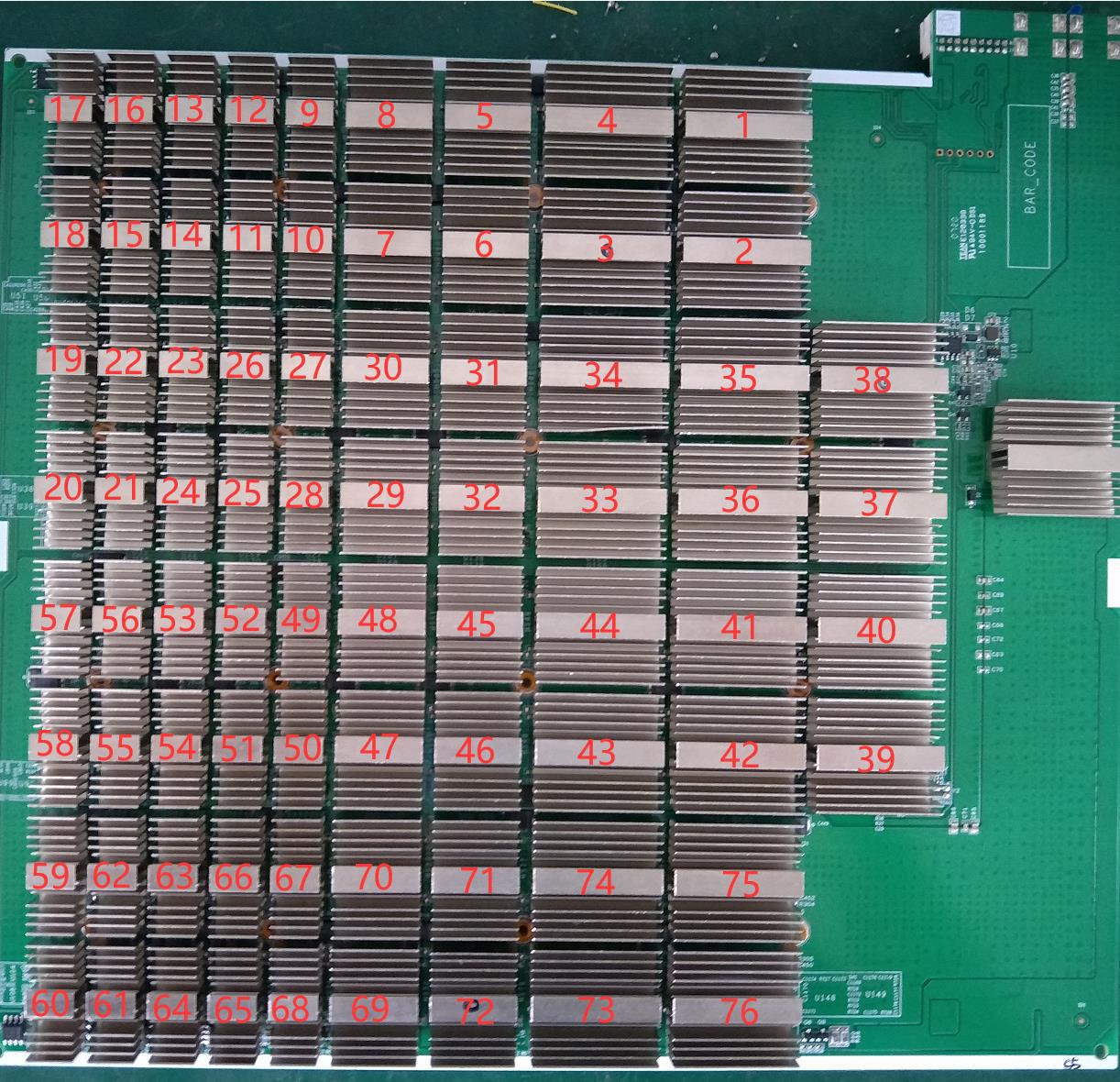
Figure 4-4
2. S19 hashboard boost circuit:
The boost circuit transfers the 14V powered by the power supply to 19V, as shown in Figure 4-5.
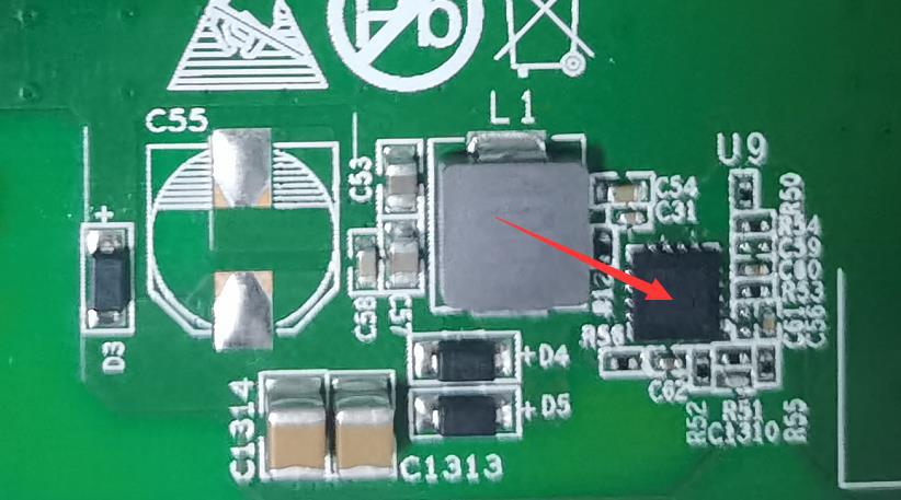
Figure 4-5
3. Signal trend of S19 chip:
1) CLK (XIN) signal flow direction, generated by Y1 25M oscillator, transmitting from chip 01 to chip 76; voltage of 0.7V-1.3V;
2) TX (CI, CO) signal flow direction, from IO port 7 pin (3.3V) into IC U2 through level conversion, and then transmitted from chip 01 to chip 76; the voltage is 0V when the IO signal is not inserted, and the voltage is 1.8V during operation;
3) RX (RI, RO) signal flow direction, from chip 76 to chip 01, return to the signal cable terminal pin 8 through U1 and then return to the control board; when the IO signal is not inserted, the voltage is 0.3V, and the voltage will be 1.8V during computing;
4) BO (BI, BO) signal flow direction, from chip 01 to chip 76; the multimeter measurement value is 0V;
5) The RST signal flow is from pin 3 of the IO port, and then is transmitted from chip 01 to chip 76; if no IO signal is inserted and equipment is in standby, voltage is 0V, 1.8V when computing;
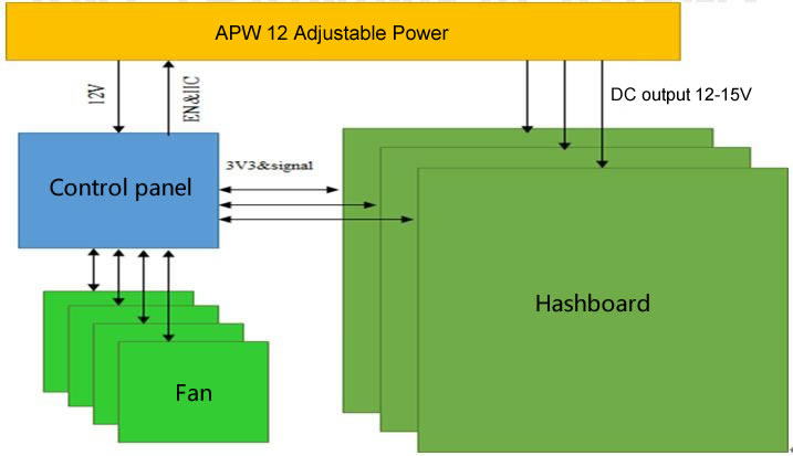
4. Whole machine architecture:
The whole machine is mainly composed of 3 hashboards, 1 control board, APW12 power supply, and 4 cooling fans, as shown in Figure 4-6.
 V. Common faults and troubleshooting steps of the hashboard
1. Phenomenon: single board test detection chip is 0 (PT1/PT2 stations)
V. Common faults and troubleshooting steps of the hashboard
1. Phenomenon: single board test detection chip is 0 (PT1/PT2 stations)
First step: check the power output first, please check the circled part in Figure 5-1.
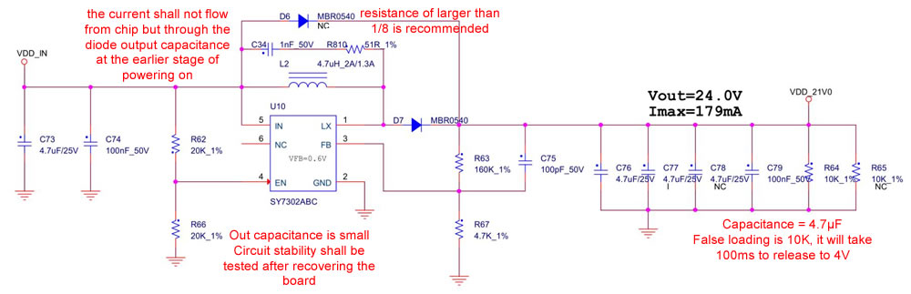
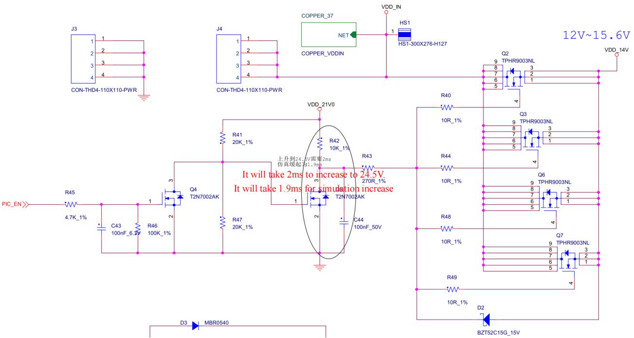
Figure 5-1
Second step: to check the voltage output in the voltage domain
The voltage of each voltage domain is about 0.36V. If there is 14V power supply, generally it has domain voltage. The priority is given to measure the output of the power supply terminal of the hashboard and whether the MOS is short-circuited (measure the resistance between pins 1, 4 and 8). If 14V has power supply but no domain voltage, continue to check.

Figure 5-2
Third step: to check the PIC circuit
Measure whether there is output on the second pin of U3 and the voltage is about 3.3V; if yes, please continue to troubleshoot the problem; if there is no 3.3V, please check the connection status of the hashboard tester cable and the hashboard is OK, and reprogram the PIC.
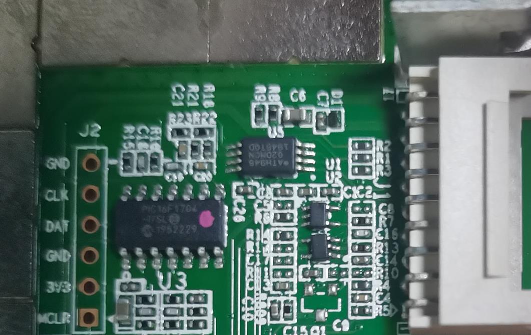
Figure 5-3
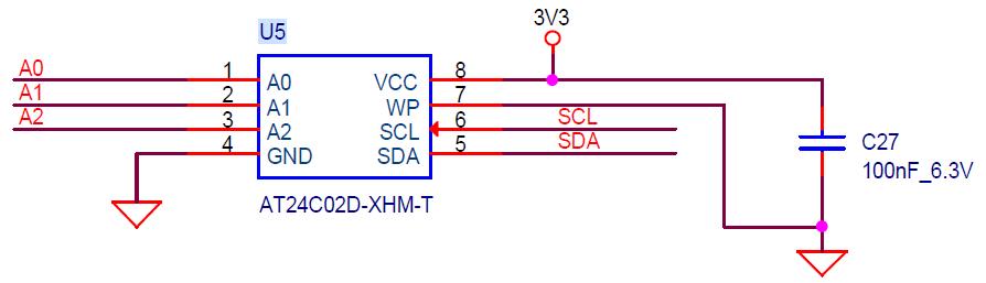
Figure 5-4

Figure 5-5
PIC programming steps:
1. PIC program programming on the hashboard.
Program: 20200101-PIC1704-BM1398-V89.hex
Download the programming tool: PICkit3, pin 1 of the PICkit3 cable corresponds to pin 1 of J3 on the PCB, and pins 1, 2, 3, 4, 5, and 6 need to be connected.
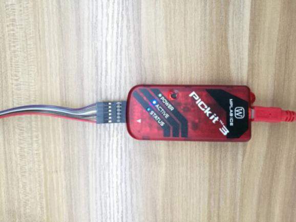
Figure 5-6
2. Programming software:
Open MPLABIPE and select device: PIC16F1704, click power to select the power supply mode, then click operate. The first step: select file to find the .HEX file to be programmed; the second step: click connect to connect normally; the third step: click the program button, and after completion, click verifiy to prompt the verification to prove that the programming is successful.
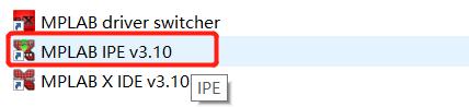
Figure 5-7
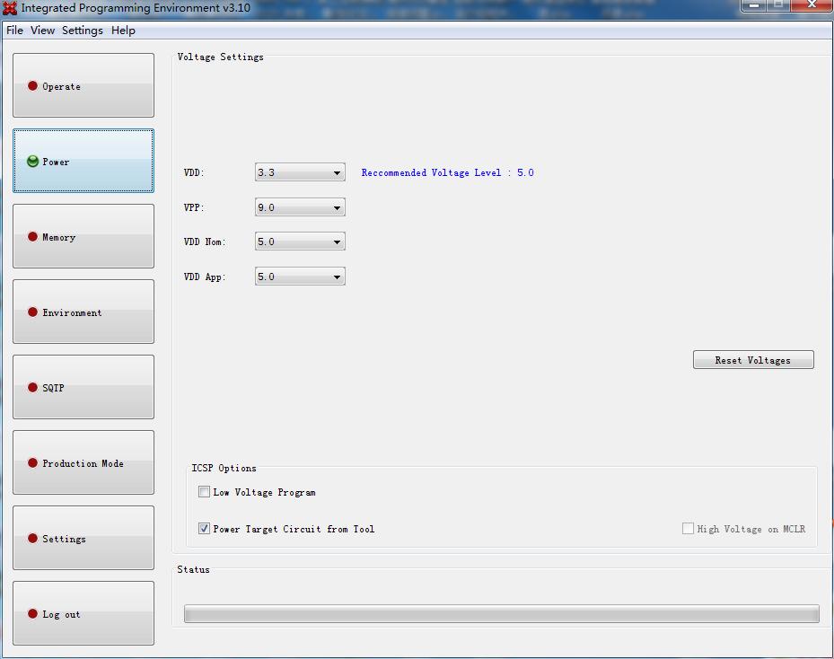

Figure 5-8
Forth step: check the boost circuit output
C55 in the test diagram 4-9 can measure 19V voltage.
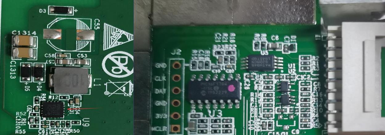
Figure 5-9
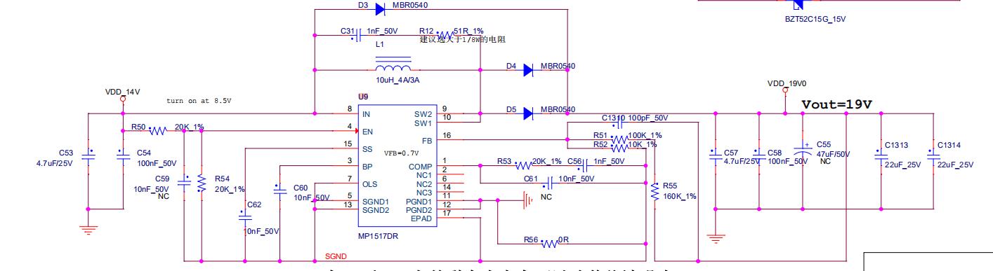
Figure 5-10
Fifth step: check the output of each group of LDO 1.8V or PLL 0.8V
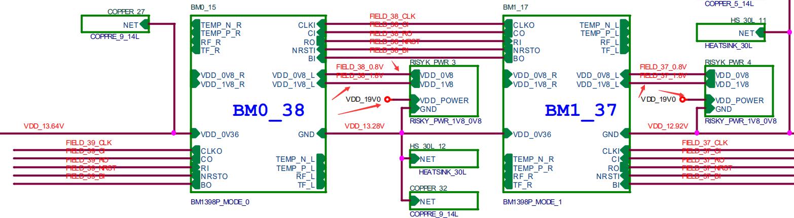

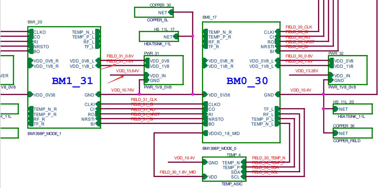
Figure 5-11
Sixth step: check the chip signal output (CLK/CI/RI/BO/RST)
1. Refer to the voltage value range described by the signal trend. If the measurement encounters a large deviation of the voltage value, it can be compared with the measured value of the adjacent group to determine.
PS: If the hashboard is not powered or powered off according to the test sequence, causing R8, R9, U1, and U2 to burn out, the chip will report 0;
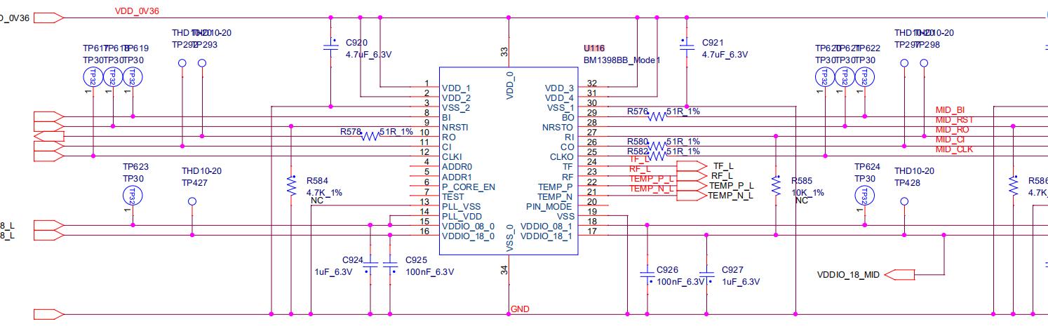
Figure 5-12
2. When the EEPROM NG is displayed on the LCD screen of the hashboard tester, check whether the welding of U5 is normal;
3. If the PICsensorNG is displayed on the LCD screen of the hashboard tester and the test read temperature is abnormal, then follow the steps below to troubleshoot:
A) Check whether the 4 resistors of R24~R27 are welding abnormally, and check whether the welding of PIN2, 3 of U3 is normal;
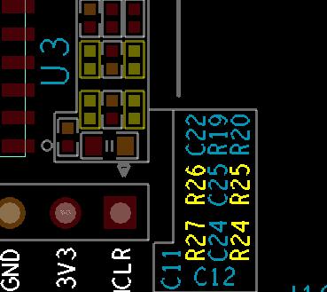
Figure 5-13
B) Check whether the four temperature senses U4, R28~R30, U6, R31~R33, U7, R34~R36, U8, R37~R39 and the matching resistance welding are abnormal, the location of the temperature sense is shown in Figure 5-14, the temperature sense is all located on the back of the PCB, the resistance is located on the front of the PCB, and whether the temperature-sensitive 3.3V power supply is normal;
Check the welding quality of the heat-sensitive chip and the small heat sink. The deformation of the large heat sink material will cause poor heat dissipation of the chip and affect the temperature difference.
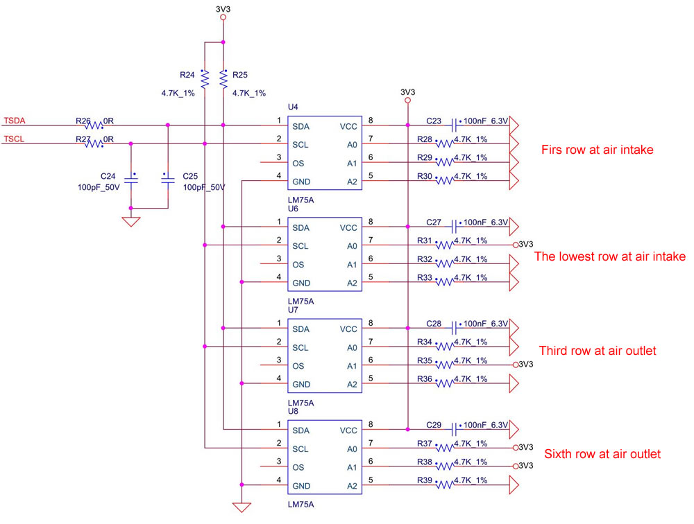
Figure 5-14
4. Phenomenon: Single board detection chip is not complete (PT1/PT2 stations)
a) LCD display ASICNG: if (0), first measure the total voltage of the measuring domain and the boost circuit 19V is normal, and then use the short-circuit probe to short-circuit the RO test point and the 1V8 test point between the first and the second chip, and then operate the program to find the chip. Looking at the serial port log, if 0 chip is still found at this time, it will be one of the following situations:
a-1) Use a multimeter to measure whether the voltages at the 1V8 and 0V8 test points are 1.8V or 0.8V. If not, it indicates that the 1.8V or 0.8V LDO circuit of this domain is abnormal, or the two ASIC chips of this domain is not soldered well; most of this are caused by short circuits of 0.8V, 1.8V patch filter capacitors (measure the resistance of the patch filter capacitors related to the front and back of the PCBA)
a-2) Check whether the circuits of U1 and U2 are abnormal, such as resistance welding, etc.
a-3) Measure the resistance of R8 or R9 with a multimeter to check if it is within 10 ohms and the reading will not jump randomly. If not, please replace these two resistors
a-4) Check if the pins of the first chip are not soldered well (it was found in repair that the pins are tinned observing from the side, but the pins are not stained with tin at all when the chip is removed)
b) If one chip can be found in step a), it indicates that the first chip and the previous circuit are good. Use a similar method to check the subsequent chips. For example, short-circuit the 1V8 test point and the RO test point between the 38th and 39th chips. If the log can find 38 chips, the first 38 chips have no problem; if you still find 0 chips, check the 1V8 first; if it's normal, it means that there is a problem with the chip after 38. Continue to investigate with dichotomy until the problematic chip is found. Assuming that there is a problem with the Nth chip, when the 1V8 and RO between the N-1th and Nth chips are short-circuited, N-1 chips can be found, but when the 1V8 and RO between the Nth and N+1th chips are short circuited, the entire chip cannot be found.
c) LCD display ASIC75: (Reporting 75), it means that the hashboard can detect 76 chips at 115200 baud rate, but only 75 chips are found at 12M baud rate, and one chip could not find at 12M baud rate;
Repair method: Using the dichotomy method, short-circuit the 1V8 test point and the RO test point between the 38th and 39th chips through the short-circuit probe. If the log can find 38 chips, there is no problem with the first 38 chips; if short-circuiting 47 chips, but the log reports 46, it indicates that the 47th chip cannot be detected, and there is no problem with the visual inspection. Generally, the 47th chip shall be replaced;
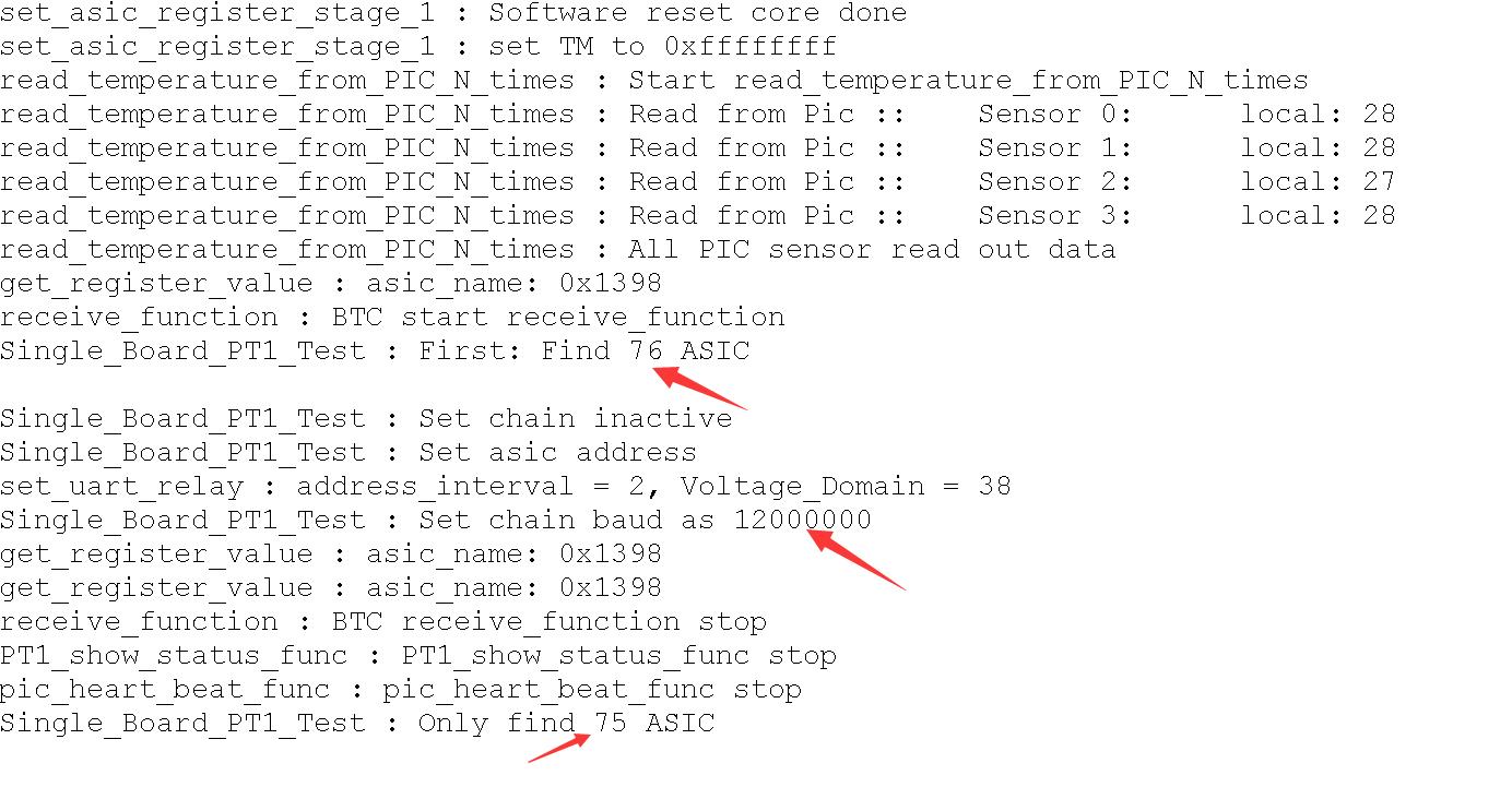
Figure 5-15
d) LCD display ASICNG: (X, a certain chip is fixed), there are two situations:
d-1) The first case: the test time is basically the same as the good board (usually the value of X will not change each time you test) (test time refers to the time from when the start test button is pressed to the result of ASICNG: (X) displayed on the LCD). This situation is likely to be caused by the abnormal resistance welding of the front and rear CLK, CI, and BO of the Xth chip, so users shall focus on these 6 resistors. The small probability is due to X-1, X, X+1, that is, among the three chips, the following pins abnormal welding conditions of the chip occur:

Figure 5-16
d-2) The second case; the test time is almost twice as long as the good board (sometimes the value of X will change every time you test, and sometimes X=0); at this time, the log usually has the following information (the red number is not 13, depending on which seat the hashboard tester is connected to); during the test, assume that the domain voltage of all the fields in front of the abnormal position is almost less than 0.3V, and the domain voltage of the back fields are almost all higher than 0.38V. This situation is caused by the chip not being soldered well, usually 1.8V, 0.8V, RXT, CLK are not soldered well. It is recommended to directly measure the domain voltage to locate which domain is the problem. The 1V8 and RO short-circuit method used in section a) can also locate the abnormal position;
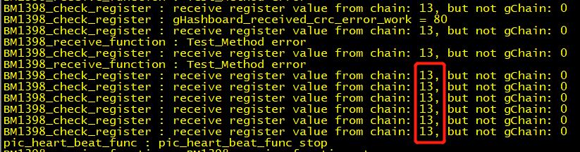
Figure 5-17
5. Phenomenon: Single board Pattern NG, indicating that the response nonce data is incomplete (PT2 station)
PatternNG is caused by the large difference between the characteristics of the chip and other chips. At present, it is found that the chip die is damaged, so just replace the chip. According to the log information, the replacement rules are as follows:
If the appearance of the chip is not damaged, just replace the chip with the lowest response rate in each domain. The following figure shows one of the test logs, it can be seen from the log that the response rate of four chips asic[36][37][43][75] is low. 36 and 37 are in the same domain, so replace the one with the lower nonce in 36 and 37. At the same time, replace the 43 and 75.
PS: Special attention shall be paid to that the numbers of domain and asic start from 0
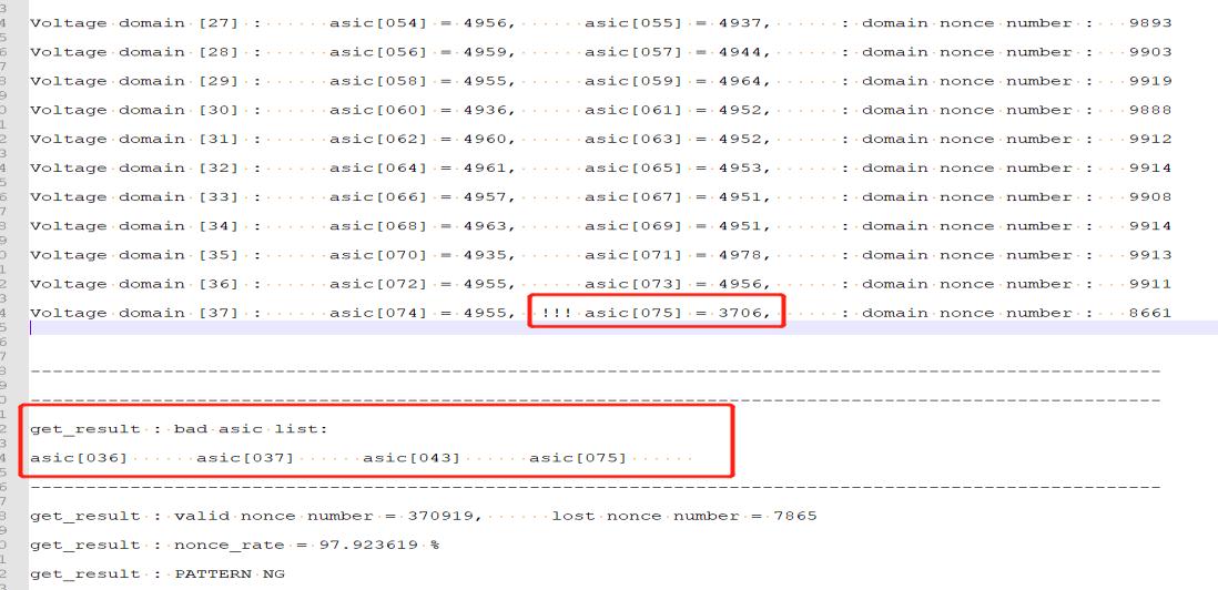
Figure 5-18
6. Phenomenon: Check that chip test is OK, PT2 function test serial port does not stop (long-distance running)
Repair method: during the PT2 test, watch the serial port print log. When the serial port starts to operate for a long time, use a short-circuit probe to short-circuit RO&1.8V. The short-circuit starts from the first chip. If the serial port stops long-tem operating after the short circuit, the first chip is OK. According to this method, find the chip that still has the long-tem operating failure after a certain chip is short�circuited. Generally, it is caused by a certain chip damaging, so just replace it;
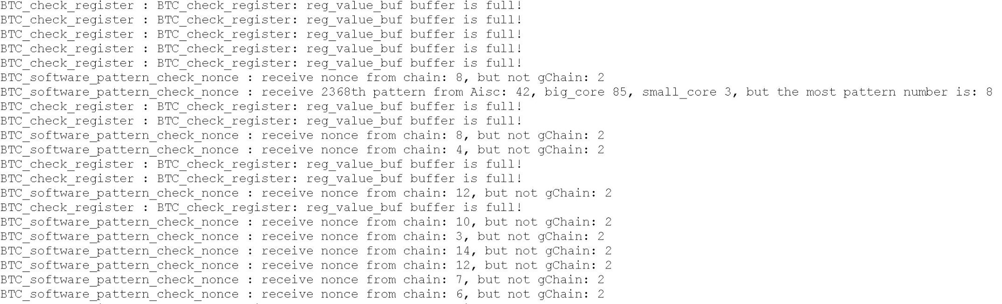
Figure 5-19
7. Phenomenon: PT1 chip test is OK, PT2 function test always reports a certain chip NG;
Repair method: check the appearance, measure the chip capacitor or resistance in front, usually it's caused by poor chip soldering or a chip capacitor, resistor damaging or abnormal resistance;
VI. Control board problem causing the following problems
1. The whole machine does not operate
1) Check whether the voltages at several voltage output points are normal. U8 can be disconnected first if 3.3V is short-circuited. If it is still short-circuited, the CPU can be unplugged for measurement. For other voltage abnormalities, generally replace the corresponding converter IC.
2) If the voltage is normal, please check the welding status of the DDR/CPU
3) Try to update the flash program with SD card;If the control board card recovery machine needs to start normally, the following two steps are required:
a) After the card recovery is successfully, the green LED indicator will be always on, and the power shall be turned off and restarted;
b) Wait for 30s after powering on again (the time course of turning on OTP)
c) OTP (One Time Programable) is a memory type of MCU, which means one-time programmable: after the program is programmed into the IC, it cannot be changed and cleared again;
Precautions:
(1) Sudden power failure during OTP or time of less than 30s will cause the control board to fail to open the OTP function. As for the issue that the control board cannot start (not networked), the user needs to replace the U1 (main control IC FBGA of control board). U1 can no longer be used in 19 series after replacement
(2) For the control board with OTP function turned on, U1 cannot be used on other series of models;
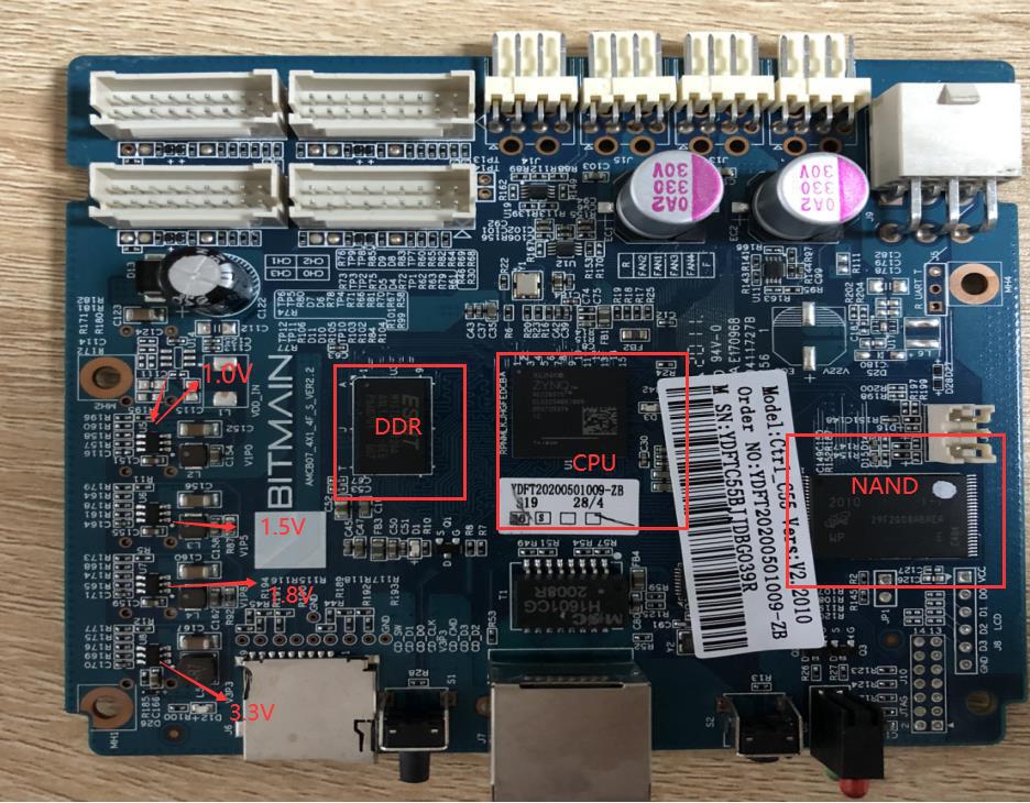
Figure 6-1
2. The whole machine cannot find the IP
Probably, the IP cannot be found due to abnormal operation. Refer to the first point for troubleshooting.
Check the appearance and welding of the network port, network transformer T1, and CPU.
3. The whole machine cannot be upgraded
Check the appearance and welding of the network port, network transformer T1, and CPU.
4. The whole machine fails to read the hashboard or has less links
A. Check the cable connection status.
B. Check the parts of the control board corresponding to the chain.
C. Check the wave soldering quality of the plug-in pins and the resistance around the plug-in interface.
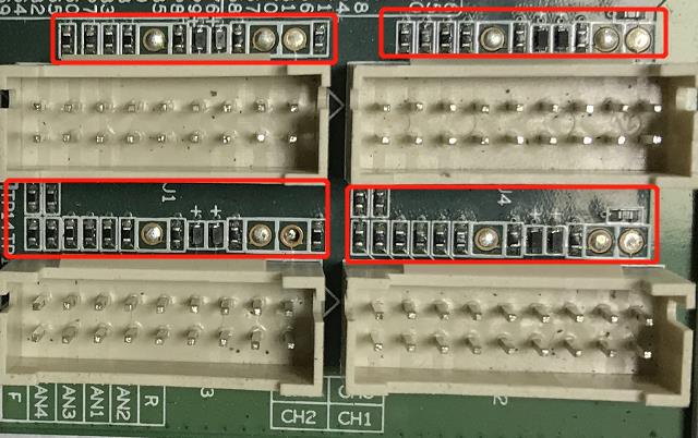
Figure 6-2
VII. Failure phenomenon of the whole machine
1. Whole machine test
Common phenomena: IP cannot be detected, the number of fans is abnormal, and the chain is abnormal. If there is an abnormality in the test, follow the monitoring interface and test LOG prompts for maintenance.
1) Fan display is abnormal - we need to check whether the fan is working normally, whether the connection with the control board is normal, and whether the control board is abnormal.
2) Less link: Less link refers to that among the 3 boards, 1 piece is missing. In most cases, there is a problem with the connection between the hashboard and the control board. Check the cable to see if there is an open circuit. If the connection is OK, the user can test the single board PT2 to check if it can pass the test. If it passes the test, it can basically be determined that the problem is on the control board. If the test fails, use the PT2 repair method to repair it.
3) Abnormal temperature: Generally, it's due to the temperature is high. The PCB temperature set by our monitoring system cannot exceed 90 degrees. If it exceeds 90 degrees, the machine will alarm and fail to work normally. It is usually caused by high ambient temperature and abnormal fan operation for the machine to not be able to work normally. Abnormal fans operation will also cause abnormal temperature.
4) Cannot find all the chips (boot can be operated, but the computing power is 2/3 or 1/3 of the normal value). The number of chips is not enough: if the number of chips is not enough, you can refer to PT2 for testing and repair.

Figure 6-4
5) After operating for a period of time, there is no computing power, the connection to the mining pool is interrupted, then check the network;
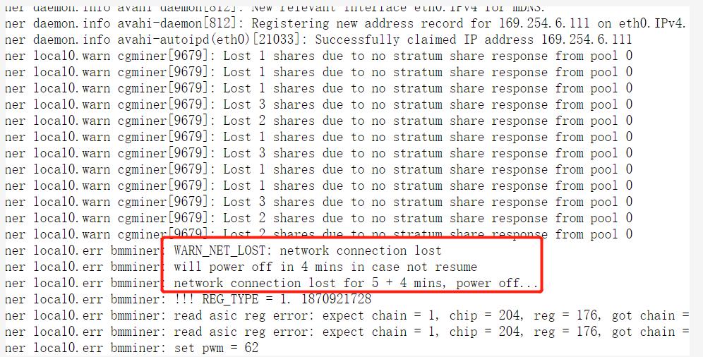
Figure 6-5
6) Test status of normal machine;
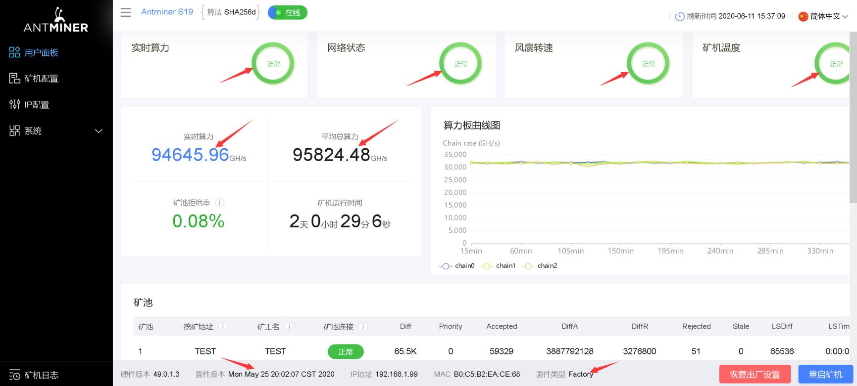 Figure 6-6
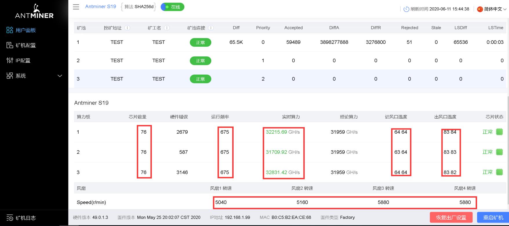
Figure 6-7
7) One hashboard has low computing power: As for this situation, you can log in to the IP through the Putty software to observe whether the domain working voltage of this board and the NONCE return are normal. You can repair it according to Putty LOG prompt.
8) How to use 'putty': tail-f /tmp/nonce.log-NONCE print command tail -f /tmp/adc.log-domain voltage print command
The specific operations are as follows:
1. Open 'putty', enter the IP of the machine in question and click OPEN.
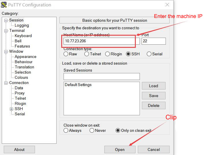
Figure 6-7
2. Enter the user name, password and test command to check the NONCE response status and the status of voltage domain. If the NONCE and domain voltage are abnormal, user can perform measurement and maintenance based on the printed abnormal chip.
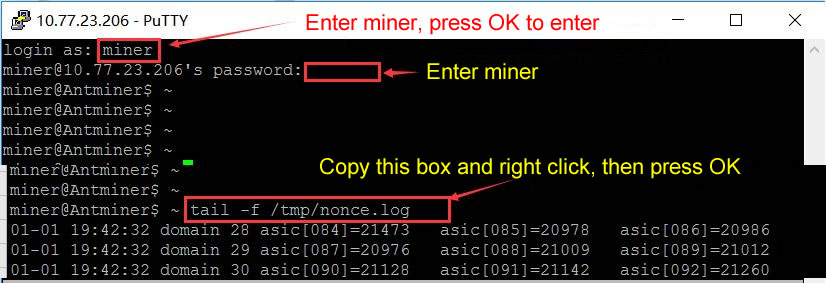
Figure 6-8
VIII. Other matters needing attention
Maintenance flowchart
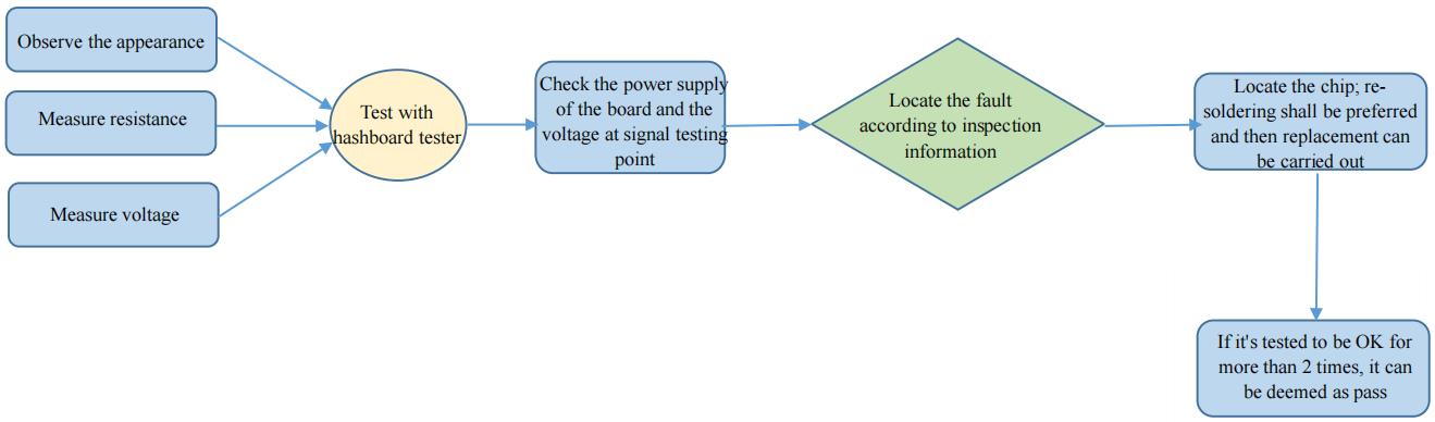
Figure 8-1 Maintenance flowchart
● Routine inspection: First, visually inspect the hashboard to be repaired, observe whether there is PCB deformation or scorching. If yes, it must be processed first; whether there are obvious burnt marks on the parts, offset parts or missing parts, etc.; secondly, after the visual inspection is passed, the impedance of each voltage domain can be tested first to detect whether there is a short circuit or an open circuit. If found, it must be dealt with first. Furthermore, check whether the voltage of each domain is about 0.36V.
● After the routine test is passed (the short-circuit test of the general routine test is necessary to avoid the chip or other materials being burnt due to the short circuit when the power is turned on), the chip test can be performed with the hashboard tester, and the positioning can be determined according to the test result of the hashboard tester.
● According to the displayed results of the hashboard tester detection, starting from near faulty chip, check the chip test points (CO/NRST/RO/XIN/BI) and voltages such as VDD0V8 and VDD1V8.
● According to the signal flow, except for the RX signal, reversely transmit the signal (from No. 76 to No. 1 chip), several of the signals including CLK CO BO RST are forward transmission (1-76), and the abnormal fault point can be found through the power supply sequence.
● When locating the faulty chip, the chip needs to be welded again. The method is to add flux around the chip (preferably no-clean flux), and heat the solder joints of the chip pins to a dissolved state to prompt the chip pins and pads to re-run in and collect the tin, so as to achieve the effect of tinning again. If the fault remains the same after re-soldering, you can directly replace the chip.
● The repaired hashboard can be judged as a good product with more than two passes when testing with the hashboard tester. For the first time, after replacing the parts, wait for the computing board to cool down, use the hashboard tester to test, and after the test is passed, set it aside and then cool it down. For the second time, after a few minutes when the hashboard cools down, test again.
Previous
Antminer S17e Hash Board Repair Manual
Read More
Next
Antminer/Whatsminer PSU Wake-up/Startup Tester Manual
Read More


 Figure 6-6


