Antminer S17e Hash Board Repair Manual
By THANOS MINING
December 17th, 2020
Mainly tells how to Bitmain Antminer S17e Troubleshoot various faults on the computing board, and explains how to use the Antminer test fixture sold by ThanosMining for accurate positioning.
New version of test fixture: Antminer S17e test fixture
I. Maintenance platform requirements
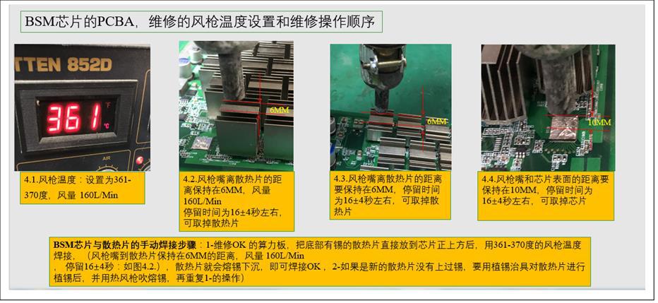
1. Constant temperature soldering iron (soldering temperature is 300‑350 degrees) pointed soldering iron tip is used for soldering small patches such as chip resistors and capacitors.
2. The hot air cylinder is used for chip disassembly and welding. Be careful not to heat it for a long time to avoid PCB blistering.
3. APW9+ power supply (output 14..5V‑21V), used for the test and measurement of the arithmetic board.
4. Multimeter, tweezers, S17e‑v1.0 test fixture (conditionally configurable oscilloscope) .
5. Flux, plate washer water plus absolute alcohol; plate washer water is used to clean up the flux residue and appearance after maintenance.
6. Tin planting fixture, planting tin steel mesh, solder paste; when replacing a new chip, you must plant the chip with tin.
7. Lead‑free alpha low temperature solder paste (OM550‑151 degrees melting point) , Used for welding heat sink after repair.
II. Job requirements
1. The maintenance personnel must have certain electronic knowledge, more than one year of maintenance experience, and be proficient in QFN package soldering technology.
2. After repairing, the computing board must be tested for more than two times and it is OK before it can pass!
3. Pay attention to the operation method when replacing the chip, there is no obvious deformation of the PCB board after replacing any accessories, check the replacement parts and whether there are few open circuits around them short circuit problem.
4. Determine the maintenance station object and the corresponding test software parameters and test fixtures.
5. Check whether the tools and fixtures can work normally.
 III. Principle and structure
Principle overview:
III. Principle and structure
Principle overview:
S17e is composed of 15 voltage domains in series, each voltage domain has 9 BM1396 chips, and the whole board has a total of 135 BM1396 chips.
1. The BM1396 chip has a built‑in step‑down diode, and the one with a step‑down diode function is determined by the specified pin of the chip.
2. BM1396 has 15 voltage domains; the S17e clock is a 25M single crystal oscillator, which is transmitted in series from the first chip to the last chip.
3. Each S17e chip has independent small heat sinks on the front and back. The front heat sink is SMT patch, and the back heat sink is after the initial test of the board. It is fixed by solder paste on the back of the IC. After the repair and replacement chip has passed the test, it needs to be soldered and fixed on the IC surface again.
Have to be aware of is:
1. In the repair process, when replacing the electrical board components or chips, in order to reduce the damage to the PCB board and the chip due to the high temperature of the air gun, The small heat sink near the faulty component and the small heat sink on the back of the PCB must be removed before replacement.
2. There are test points on the front and back of the PCB. For maintenance during production, when the heat sink is not attached to the front of the PCB, the front test point can be used; the finished product is repaired (After‑sales maintenance), since the front and back sides of the PCB are covered with heat sinks, it is necessary to locate the fault through the test points of the PCB. Specially made The long and slender test lead probes into the gap of the heat sink for measurement, but since the small SMT heat sink is connected to the ground of each voltage domain, pay attention when measuring insulate the test leads to avoid short circuit caused by the test leads.
Key point analysis :
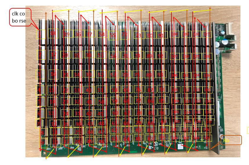
Figure 1 , Signal trend
The picture above shows the signal trend of S17e
Red is the flow of CLK signal, generated by Y1 25M crystal oscillator, transmitted from chip 1 to chip 135; standby and operation When the voltage is 0.8±0.1V.
Red is the direction of TX (CI, CO) signal flow, which enters from pin 7 of IO port, and then transmits from chip 01 to chip 135; not inserted The voltage of the IO line is 0, and the voltage of the calculation is 1.8V.
Yellow is the direction of RX (RI, RO) signal flow, from chip 135 to chip 00, then return to control from IO port 8 Board; when the IO signal is not inserted, the voltage is 1.8V, and the voltage is also 1.8V during calculation.
Red is the signal flow direction of B (BI, BO), which is pulled low from chip 00 to 135; when the IO line is not inserted, it is 0V when in standby, It is a pulse signal of about 0.3 during calculation.
Red is the flow direction of RST signal, which enters from pin 3 of IO port, and then transmits from chip 00 to chip 135; without IO signal inserted, it is 0V in standby mode, and 1.8V in operation.
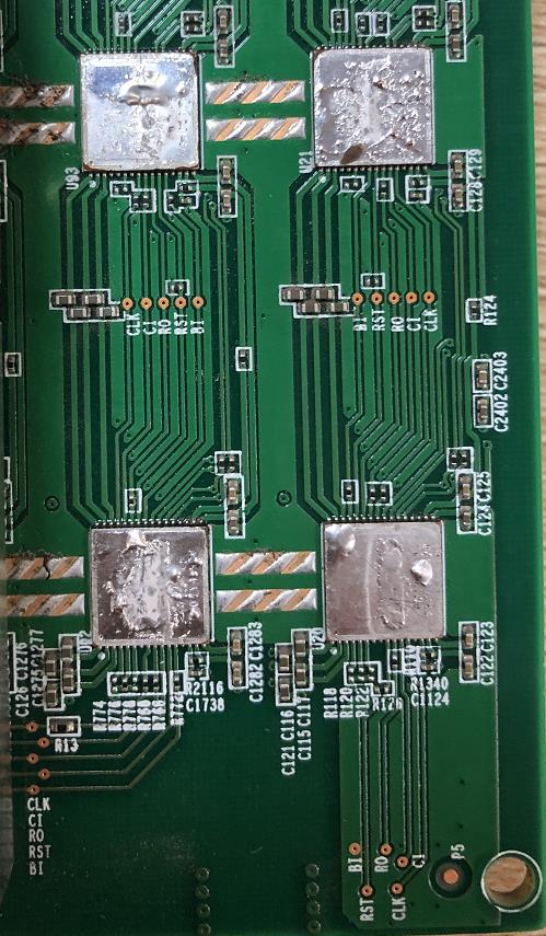
Figure 3 shows the key circuits on the front of the T arithmetic board.
1. Test points between each chip (as shown in the figure after zooming in): Figure 2
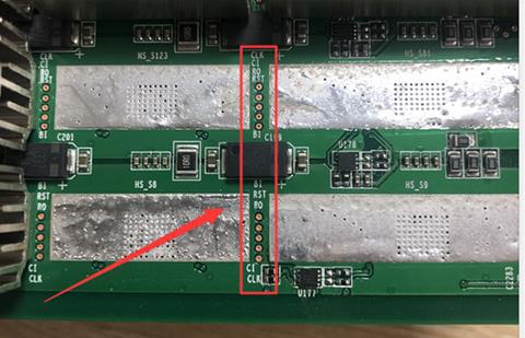
Figure 2 , Test points between chips
When repairing, the test points between test chips are the most direct
Fault location method. The arrangement of the test points of the S17e computing board is: As shown on the left
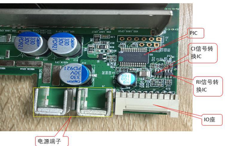
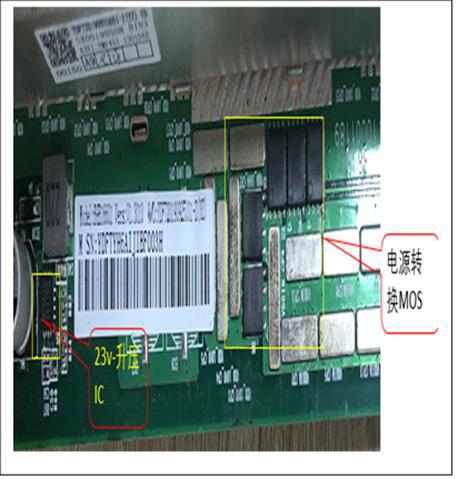
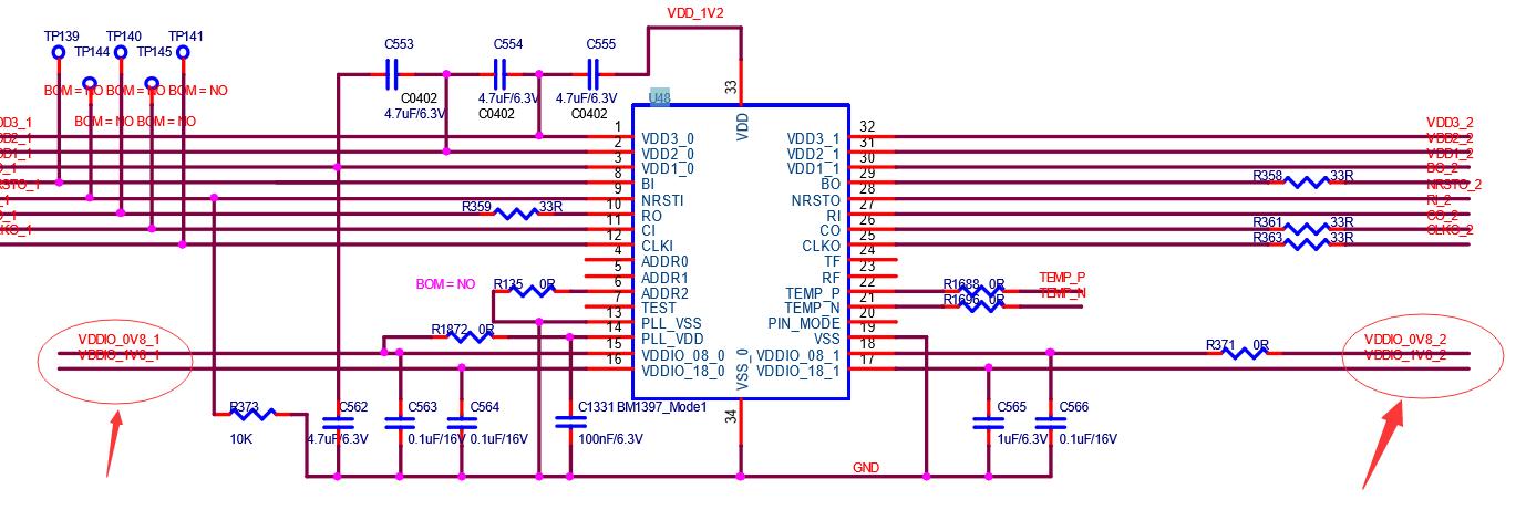
Figure 3 , S17e The key circuits on the front of the operation board
3. Voltage domain: The whole board has 15 voltage domains, and each voltage has 9 chips. The total voltage domain voltage is 18V. The voltage of each voltage domain is 1.2V. The 9 chips in the same voltage domain are powered in parallel, and then connected in series with other voltage domains after being connected in parallel. The circuit structure is shown in Figure 4 below:
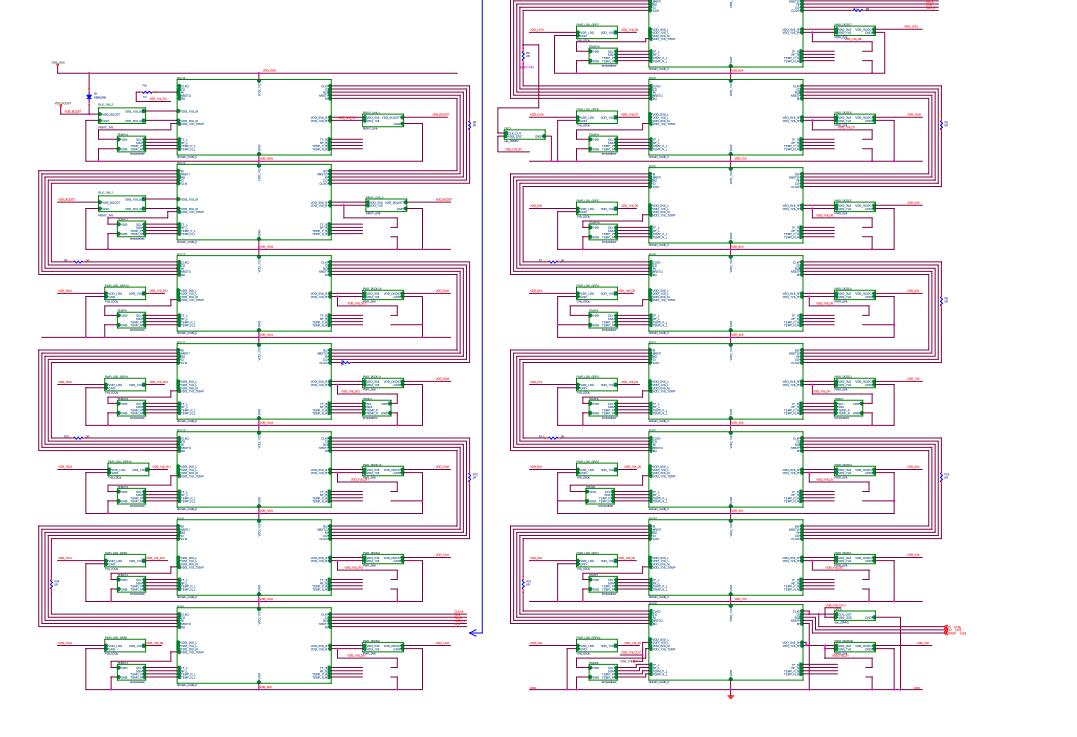
Figure 4 Yes S17e The key circuits on the front of the operation board
Principle analysis of voltage domain single chip (as shown in Figure 5 and Figure 6 below):

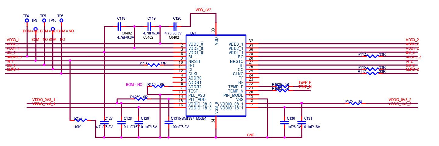
Figure 5 , BM1396 Circuit diagram
The above is the function of each pin of the BM1396 chip.
During maintenance, mainly test the test signal points before and after the chip (five before and after the chip: CLK, CO, RI, BO, RST);
Detection method:
1. When the fixture is not tested, APW9+ outputs 18.4V to power the fixture control board.
2. When the fixture starts to test, APW9+ will output 18.4V to supply positive power to the power terminal of the control board. During the test of the fixture, each
The voltages of the pilot are as follows:
CLK : 0.9V.
CO : 1.6‑1.8V, when the fixture just sends WORK, the DC level will be pulled down because the CO is negative, and the instantaneous voltage is about 1.5V.
RI :1.6‑1.8V. During calculation, the abnormal or low voltage will cause the calculation board to be abnormal or the computing power is 0.
BO :It is 0V when there is no operation, and there will be a pulse jump between 0.1‑0.3V during operation.
RST : 1.8V. Each time you press the test button of the fixture, the reset signal will be output again.
When the above‑mentioned test point status and voltage are abnormal, please estimate the fault point based on the circuit before and after the test point.
Visible from the above list:
CLK Signal: input from pin 12 of the chip and output from pin 25. When connecting across the voltage domain, it is connected from pin 8 to pin 29 of the next chip through a 0 ohm resistor connection;
TX Signal: from the chip 11 feet in, 26 feet out;
RX Signal: by the chip 10 Feet return, 27 Pin output
BO Signal: input from pin 8 of the chip and output from pin 29;
RST Signal: by the chip 9 Pin is in, 28 pin is output.
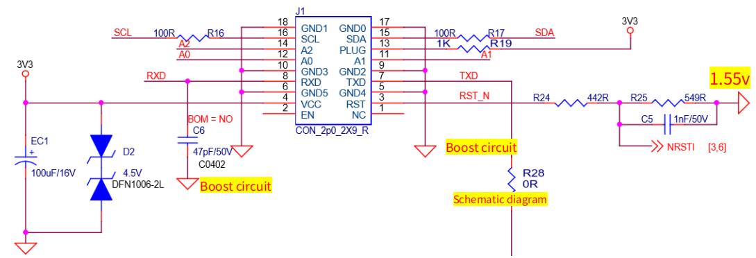
Figure 8 , IO Definition of each pin
As shown in FIG:
6, 10, 18, 5, 9, 17 feet : It is GND.
15, 16 feet (SDA, SCL) : It is the I2C bus of DC‑DC PIC, which connects the communication between the control board and the PIC. The control board can read and write data of the PIC through it, thereby controlling the operation status of its computing board.
13 Feet (PLUG0): It is the identification signal of the arithmetic board. This signal is pulled from the arithmetic board 1K resistance to 3.3V, so when the IO signal is plugged in, this pinbShould be high level.
11, 12, 14 feet (A2, A1, A0) : PIC address signal.
7, 8 feet (TXD, RXD) : It is the channel of computing power at the 3.3 end of the arithmetic board, which becomes the TX (CO) and RX (RI) signals after being divided by the resistance.
3 Feet (RST): It is the 3.3V end of the reset signal, which becomes 1.8V RST reset signal after being divided by resistors.
4 Feet (D3V3) : Supply the 3.3V power supply for the computing board. The 3.3V is provided by the control board, mainly to provide the working voltage for the PIC.
23V boost circuit:
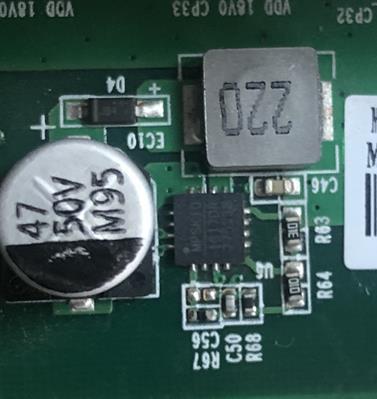
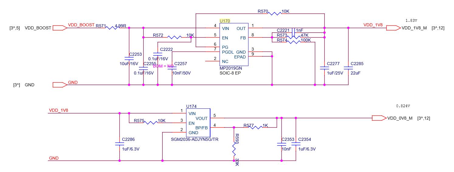
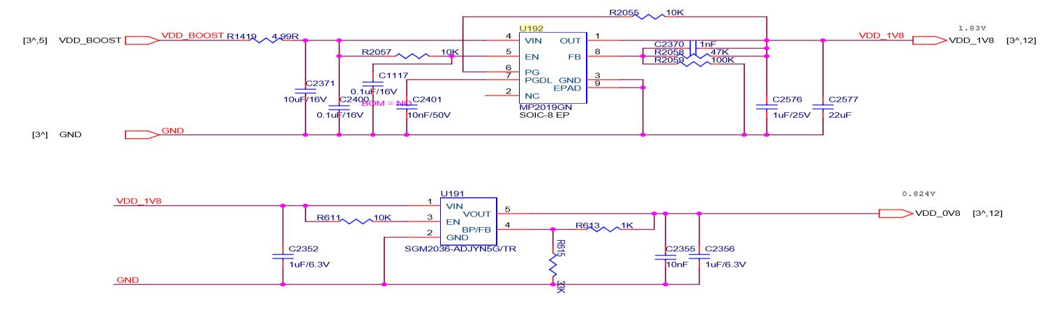
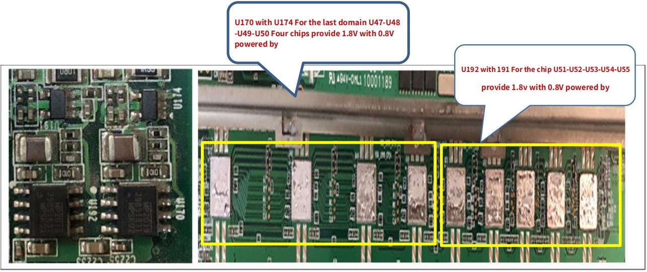
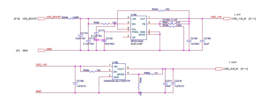
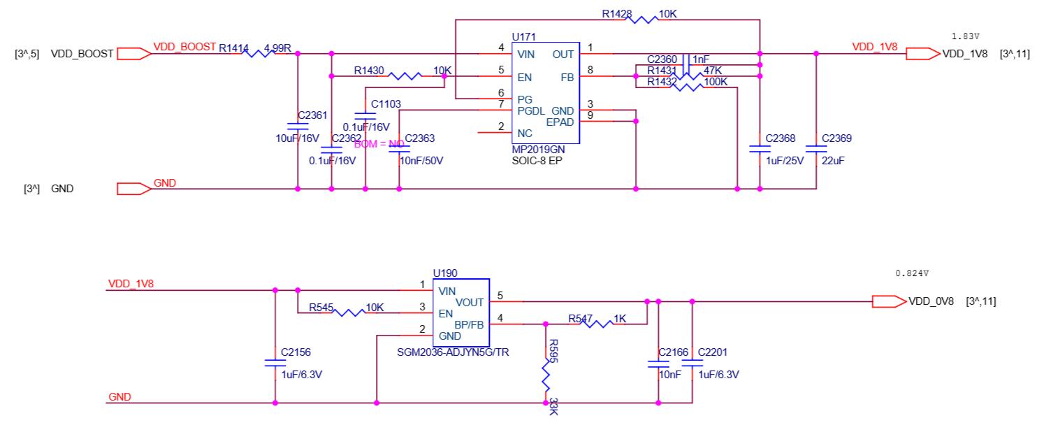
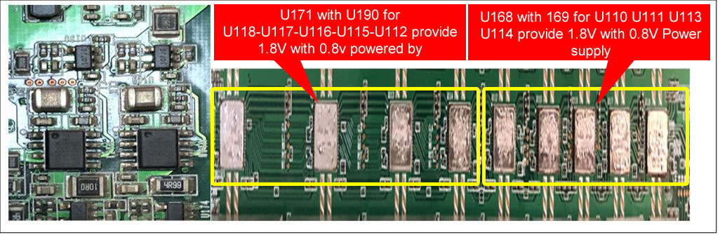
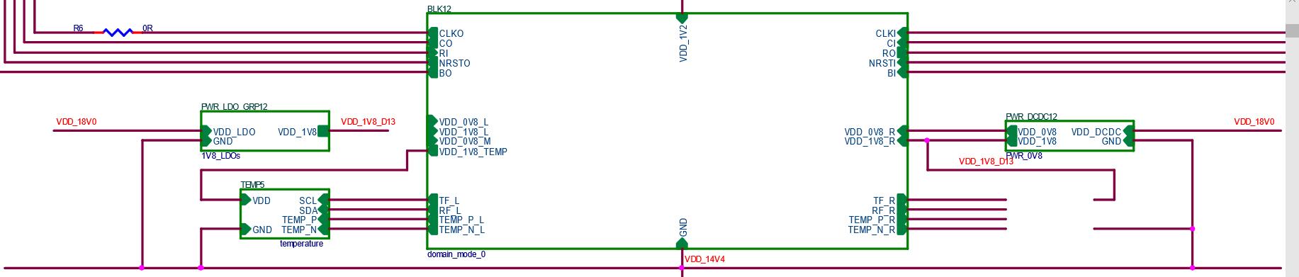
Responsible for boosting the DC‑DC (18v) to 23V. The principle is to increase the voltage of 18V to 23V through U6 L1 D4. The switching signal produced by U6 is the energy storage inductor through L1, and D4 is the boost rectifier diode to charge and discharge C47 C51 , So as to get the 23V of the positive electrode of EC10. The main 18v power supply voltage is as shown in the figure below. After U168‑U171 and U170‑U192 are stepped down, 1.8V is output to supply 1.8V to the chips in the last two domains. Pay special attention to the 1.8V output from U192 in these two domains to the chip U51 in the last domain. ‑U52‑U53‑U54‑U55's 1.8v power supply also provides 1.8V power supply for U191. Similarly, U191 outputs 0.8V and U51‑U52‑U53‑U54‑U55 provides 0.8v power supply, and U170 and U174 are the last ones. The U47‑U48‑U49‑U50 four chips of the domain provide 1.8V and 0.8V power supply. U171 and U190 provide 1.8V and 0.8V power supply for U118‑U117‑U116‑U115‑U112, and U168 and 169 provide 1.8V and 0.8V power supply for U110‑U111‑U113‑U114. The specific schematic and physical diagrams are as follows:
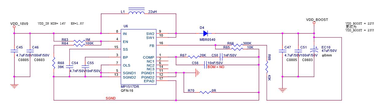
Figure 11 , 14V Boost schematic
PIC Schematic diagram
The 1.8V and 0.8V of the other voltage domains (1‑13 voltage domains) are the voltages of the three voltage domains after obtaining, each voltage domain voltage is 1.2, the three voltage domains are 3.6V, and each voltage domain has only 1 A 1.8V and 0.8V LDO powers 9 chips in a voltage domain.
DC‑PIC: Consists of PICC33EP. As shown in Figure 13, Figure 14:
The device that stores the frequency information and voltage value of the arithmetic board chip can also control the APW9+'s DC‑DC output voltage.
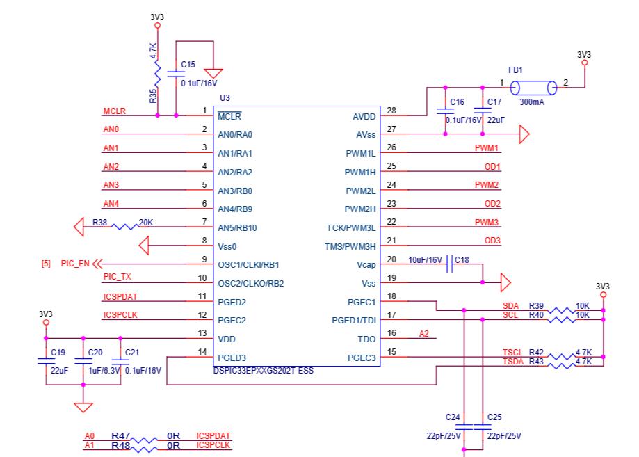
Figure 13 , PIC Schematic diagram
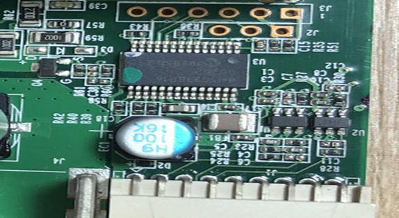
Figure 14 , PIC Circuit
PIC When working, you need to control and issue one every minute Second heartbeat signal, if there is no heartbeat information, PIC will Will work for one minute and then shut down.
DC‑DC circuit: composed of 2N7002 and CMOS tube TPHRMDU3603NL. As shown in Figure 15 and Figure 16 below: The working principle is: PIC99 pin PICEN small signal is the first level voltage of a few tenths of a volt, Q4 pin 1 is low level, Q4 is non‑conducting, Q1‑Q2‑Q4‑Q5 is 4 When the pin is high, the 4 MOS transistors will not be turned on, and the hashrate board will not have 18V power supply, On the contrary, Q4—1 pin is high level. Q4's pin 2 and pin 3 are connected to the ground, Q1‑Q2‑Q4‑Q5 turns on 18V to supply power to the hash board.
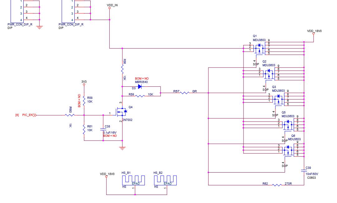
Figure 15 , DC‑DC Schematic diagram
Figure 16 , DC‑DC Physical map
25M LCK is composed of Y 25MHZ passive crystal oscillator, as shown in Figure 17 and Figure 18:
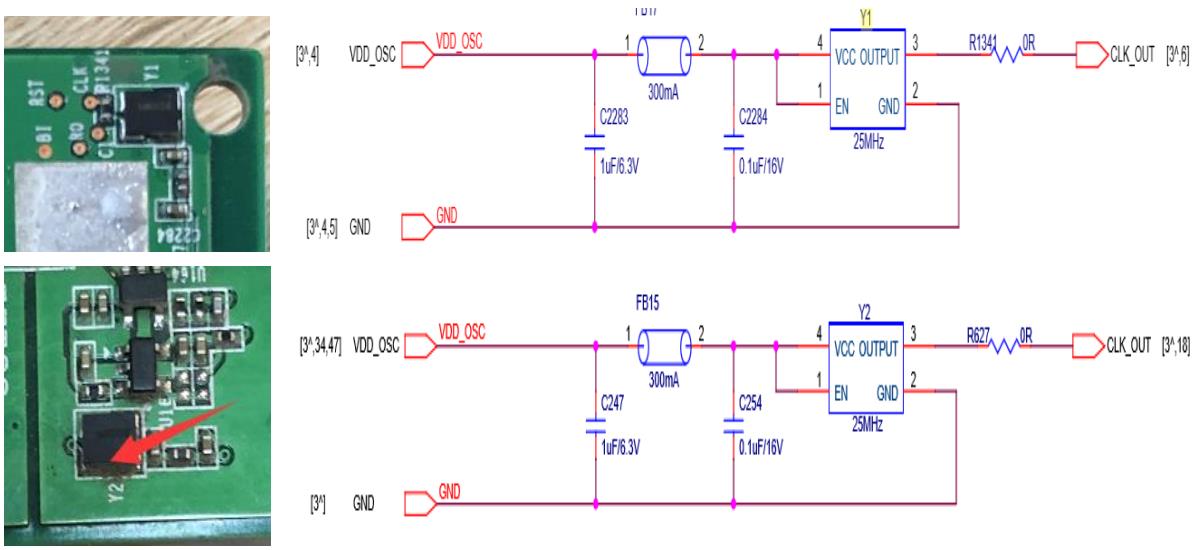
Figure 17&18 , 25M LCK principle
Normally, the voltage at both ends of R134 is about 1V.
The power supply of Y1 and Y2 powers the 1.8V‑LDO‑1.8v of this domain, and the output voltage is 0.8‑1v.
Temperature sensing circuit: There are two temperature sensing circuits, one is TEMP (PCB), this is composed of sensor IC‑U178‑TMP451; the other is TEMP (CHIP), this is the built‑in temperature sensor group (BM1396 No. 22, 21st pin), these two temperature sensing parameters are collected and finally pass through the 23rd and 24th pins of BM1396, and then return to the FPGA of the control board from the RI. The principle is shown in Figure 21: (S17E has a total of 15 temperature sensors, all of which are The chip at the end of the air outlet)
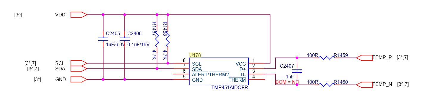

Figure twenty one , Temperature sensing principle diagram

Special attention: C118‑119‑120 on pins 0‑1‑2‑3 of the U221 chip are the 4 smaller filter capacitors inside the chip, because the height of the dot capacitance is greater than the height of the chip, it is easy to cause heat sinks and capacitors Short circuit, our 1396 chip has 3833 cores. Each chip has 4 small domains, which means that the voltage of each chip is 1.2V, and the voltage of each of the 4 small domains is 0.3V.
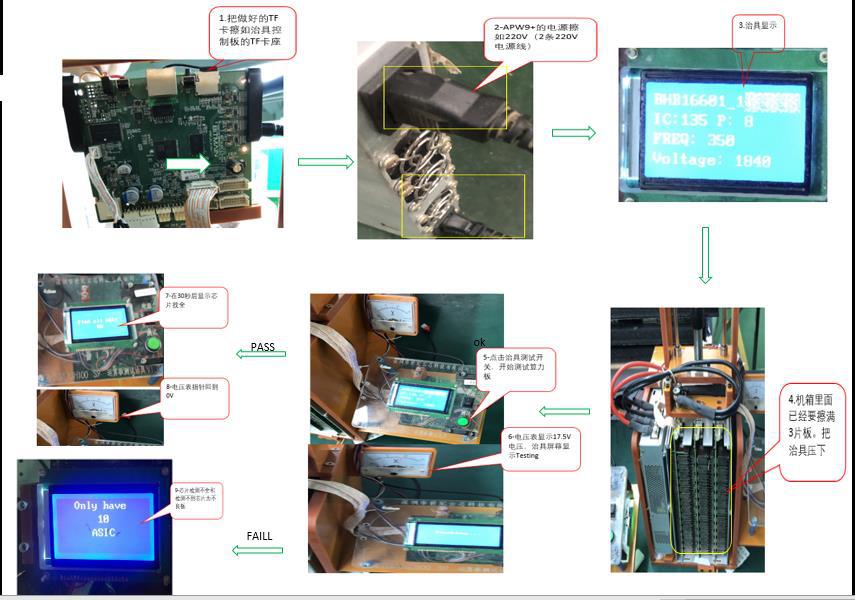
Test the production of TF card
1. Prepare a 4G or 8G TF card
2. Prepare a card reader
3. Decompress the BHB16601 test fixture
4. Unzip the folder before brushing the glue
5. Copy the decompressed file to the formatted TF card
6. Eject the TF card and test that the T card is made successfully

1. Wipe the completed TF card into the TF card socket of the fixture control board. The
2. power of APW9+ is connected to 220V power cord (2 220V power cords) .
3. The screen display after the jig is running.
4. Three boards must be inserted in the case. Press down the jig and the thimble of the jig contacts the power terminal of the hashrate board.
5. Click the fixture test switch to start testing the hash board.
6. The voltmeter displays 17.5V and the fixture screen displays Testing.
7. After 30 seconds, the screen displays the chip search (find all asic OK test time is 30 seconds). The pointer of
8. the voltmeter returns to 0V.
9. If the chip cannot be found or cannot be found, the screen will display ASIC=0 or ASIC=xx.
10. After the test is completed, you must wait for the pointer of the voltmeter to be OV, then you can separate the jig power supply thimble from the control board, take out the hash board, and mark the bad PCBA with the bad label and place it separately.
 IV. single board repair case analysis
Single board fixture test asic=0 failure analysis:
IV. single board repair case analysis
Single board fixture test asic=0 failure analysis:
1. Whether the fixture cable and the hash board are in good contact.
2. If it is S17e, the hashrate board J4‑J5 should have a voltage of 18. V during the fixture test.
3. When testing the fixture, measure whether there is voltage between 15 voltage domains.
3.1 If there is no voltage in the voltage domain, it depends on the normal working voltage of pin 4 of Q1‑2‑3‑5 that the high level is 3.3V, if it is low level, then See if pin 1 of Q4 is high at 3.3V. If Q4 does not have a 3.3V voltage, it means that U3‑PIC has lost its firmware or has no power supply.
3.2. If the power supply is normal and the voltage domain voltage is also available, then measure the RI signal of the chip to see if the RI signal has a voltage of 1.8V, and measure the RI The signal should be measured from the test point of the last chip. If the last chip is available, you can measure whether the 20th chip has RI ‑1.8v or not.
By analogy, when the chip has no RI output voltage, first measure it. The chip is powered by 1.8V. If 1.8V is not powered, then
It is necessary to check the 1.8V power supply circuit. The 1.8V power supply circuit is obtained by dividing the voltage in the voltage domain and then powering the LDO 1 pin, and the LDO 5 pin output 1.8V voltage, (each voltage domain has a ‑1.8V LDO that powers the chip) , If there is no output, there should be a problem with this LDO.
If 1.8V is normal, you can measure the resistance to ground of the test point after power off and compare it with the OK board to see if there is any abnormal resistance. If the resistance is
Normally, there is no problem with soldering. It should be that the chip is bad. (Replant the removed chip and solder it to a good board for verification. If There is no RI signal to prove that this chip is broken, just replace it with a new one)
The fault phenomenon is ASIC=7:
Analysis: ASIC=7
1. The single board test can find 7 chips. It can be judged that the RI signal is normal. If the 8th chip is not found, we will directly measure the 7th chip.
The voltage of the U26‑CLK‑RST‑CO chip depends on whether the power supply is normal. If the CLK does not have a 0.8V voltage, it depends on the power supply of the CLK Circuit.
2. 2‑CLK circuit analysis: If the CLK is not 0.8V, first look at whether the 0.8V power supply of the bad chip voltage domain is normal. The 0.8V power supply circuit is
After dividing the voltage in the voltage domain, it is the same as the 1.8V power supply. The maintenance method for the 5‑pin output 0.8V can refer to the 1.8V maintenance method.
(It should be noted that the 4 chips in each domain of S17 have 2 output 0.8V LDO power supply, and each LDO supplies 2 chips).
3. If the 0.8V power supply circuit does not have a 0.8V output, then look at whether the 0.8V LDO power supply has a power supply voltage of about 3.2V, and if so, look at it.
Whether the LDO is soldered or short‑circuited, if there is a 0.8V output, then look at the resistance of this chip to ground, if the resistance is correct, it should be the chip bad.
PATTERN‑N
For the PCBA of PATTERN‑NG, we first judge whether the chip is defective through the NONCE returned by each chip indicated by the LOG of the fixture test. If 1‑2 chips return NONCE insufficient (generally, the number of NONCE returned by a single chip is 8x383x0.98), just replace these two directly. For each chip, if it is 9 chips with a domain, the NONCE return does not reach 98%, basically it can be determined that the voltage of this domain is low.
V. Judgment criteria and failure analysis of the whole machine test
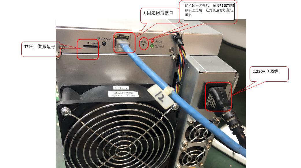
1. Connect the assembled whole machine to dual 220V power cords and fixed IP network cables (Figure 1).
2. Enter the test site monitoring interface to find the IP of the tested machine.
3. After the machine is turned on, the machine can run out of computing power in about 3 minutes.
4. After the machine runs for 10 minutes, click on IP51 to enter the mining machine interface, and then enter the IP, enter the account name root and password root to enter the mining machine IP interface
To confirm whether the firmware version date is correct.
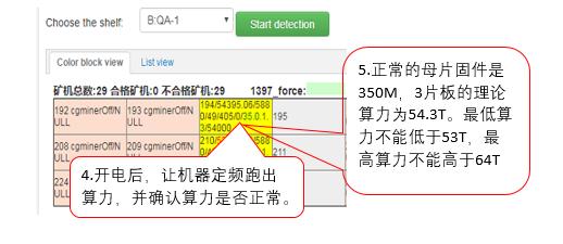
5. The normal master firmware is 300M, and the theoretical computing power of 3 boards after 10 minutes of operation is 46T. The minimum computing power cannot be lower than 98%T, the maximum computing power
It cannot be higher than 1.2T, and it is considered bad if it exceeds the maximum and minimum computing power.
6. The RT hashrate cannot be lower than 98% of the AVG hashrate and cannot be higher than 1.2.
7. The number of chains of the whole machine cannot be less than 3, the number of chips each cannot be less than 135, the frequency of each chain cannot be less than 300M, and the temperature of the PCB
It cannot be lower than 25 degrees, the temperature of the chip cannot be lower than 30 degrees, and it cannot be higher than 100 degrees. The number of fans cannot be less than 4, the speed of the fans
It cannot be less than 2000 revolutions.

Whether the whole machine is running normally depends on whether the machine can start normally and whether the computing power is normal. To check whether the computing power is normal, enter the machine first
The IP of the device is shown in the above figure.
1. Whether the number of chains has detected 3 chains: If it is not detected enough, it depends on whether the flat cable has fallen off or the flat cable has not been plugged in properly.
If it takes to update the cable or the chain is still less, you can perform a single board test on the hash board of the less chain to see if it is OK;
1.1‑ If the hashrate board is OK, it can basically be determined as the control board, and it can be eliminated by the substitution elimination method;
1.2‑ If the hashrate board tests ASIC0, then repair it according to the single board repair method;
2. Check if the number of chips is enough: If the number of chips is not enough, you can directly enter the IP‑LOG to see how many chips are detected in that chain, and then Repair according to the number of chips per board.
3. See if the operating frequency of the three chains is normal: frequency determines the computing power, one chain computing power = frequency x number of chip cores 383 x number of chips x 0.98.
If you can’t reach this theoretical computing power, it proves that the chips in this chain have a lot of bad CORE. If you want to increase the computing power, you can enter the IP‑LOG to see that.
If the frequency of the chip is lower, replace that chip.
4. Under normal machine operation, the temperature of PCB and chip of 3 chains is between 25 degrees and 95 degrees. If there is one chain, the temperature is only 25 degrees.
Below degree, it proves that the hashrate boards of this chain are not working, and the veneer test is necessary to see if the veneer is normal. If it is higher than 95 degrees, it proves heat dissipation
No, check whether the fan operation and ventilation of the machine are normal, and also pay attention to whether the heat sink has fallen off.
5. If you can't see any data after entering the IP, but only see the interface as shown in the figure below, you must enter the IP‑log to see what is printed in the log
Regardless of the information, check and repair the machine according to the information. It may be a disconnection or other problems.
6. When the whole machine is repaired, it is repaired according to the mining status and LOG, and which one is considered to be the problem is directly replaced with a good part for verification.
Make judgments.
Reference steps:
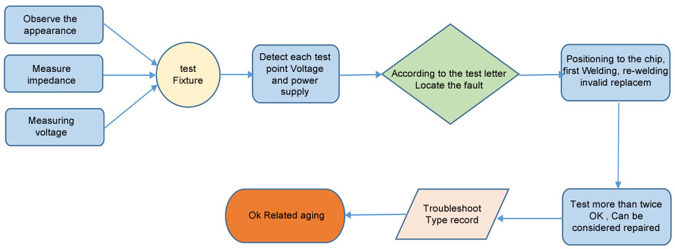
1. Routine inspection: First, visually inspect the computing board to be repaired to observe whether there is any displacement, deformation, or scorching of the small heat sink. If there is It must be dealt with first; if the small heat sink is displaced, remove it first, and then re‑soldering after the repair is passed.
Secondly, after the visual inspection is no problem, the impedance of each voltage domain can be tested first to detect whether there is a short circuit or an open circuit. If you find it, you must first OK to deal with it.
Thirdly, check whether the voltage of each voltage domain reaches 1.2v, and the voltage difference of each voltage domain shall not exceed 0.3v. The voltage of a certain voltage domain is too high or
If it is too low, the circuits in the adjacent voltage domain generally have abnormal phenomena. Need to investigate the reason first.
2. After the conventional test is no problem (Generally, the short‑circuit test of the conventional test is necessary, so as not to burn the chip or other materials due to the short circuit when the power is turned on.
Material), the chip can be tested with a test fixture, and the positioning can be judged according to the test result of the test fixture.
3. According to the displayed results of the test fixture, start from the vicinity of the faulty chip, and check the chip test points (CLK IN OUT/TX IN OUT/RX IN OUT/B IN OUT/RST IN OUT) and VDD VDD0V8 VDD1V8 and other voltages.
4. Then according to the signal flow direction, except for the RX signal, it is transmitted in the reverse direction (from 135 to chip 1), and several signals CLK CO BO RST are transmitted in the forward direction.
(1‑135, find the abnormal fault point through the power supply sequence.
5. When locating the faulty chip, the chip needs to be welded again. The method is to add flux around the chip (preferably no‑clean flux) ,will
When the solder joints of the chip pins are heated to a dissolved state, gently move up, down, left, and right to press the chip; to promote the chip pins and the pads to run in again,
Collect tin. In order to achieve the effect of tinning again.
If the fault remains the same after re‑soldering, you can directly replace the chip.
6. The repaired arithmetic board must be tested more than twice when testing the fixture. Two test times before and after: the first time, after changing the configuration
After the parts are completed, the arithmetic board needs to be cooled down, and after passing the test, put it aside; the second time, after a few minutes, wait for the arithmetic board to be completely
After cooling down, test again. Although the time interval between the two tests is a few minutes, it does not affect the work. Put the repaired board aside and continue
Repair the second board, wait for the second board to be repaired and set aside to cool down, and then test the first board. This is just a time stagger, and does not delay the total duration.
7. Classify the repaired board according to the fault, and make a record of the replacement component model, location, reason, etc., in preparation for feedback to the production and sales
Later, research and development.
8. After recording, install it into a complete machine for formal aging.
VI. the type of failure
S17e common fault types are:
1. Remove the heat sink, heat sink shift, and deformation; before power on, the heat sink on the PCB board on the back of the computing board chip is not allowed to shift or touch, especially
Don't be heat sinks of different voltages. The contact of heat sinks of different voltage domains means that there is a possibility of short circuit at different voltage points. And make sure the computing board
Each heat sink on the board has good heat conduction and is firmly fixed.
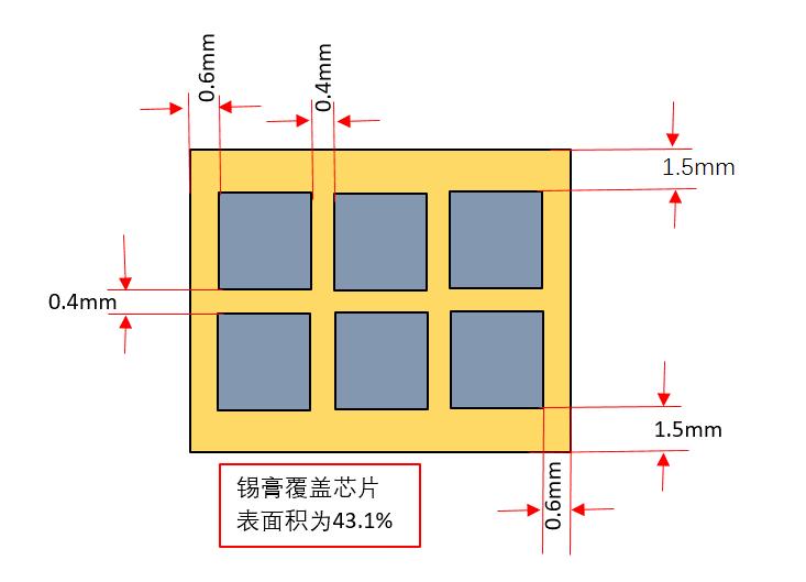
When replacing or reattaching the heat sink, you need to replant tin on the heat sink and chip before soldering. The requirement for tin planting: the thickness of the steel sheet is 0.12mm.
The area is more than 40% of the surface area of the BSM chip. details as follows:
2. The impedance of each voltage domain is unbalanced;
When the impedance of some voltage domains deviates from the normal value, it means that there are parts in the abnormal voltage domain that have open circuits or short circuits, which may be caused by general chips.
The most sex. But there are three chips in each voltage domain, and often when it fails, only one chip has the problem. The problematic chip can pass the inspection
Measure and compare each chip's test point to ground impedance to find the abnormal point.
If you encounter a short circuit, you can remove the heat sink on the chip in the same voltage domain first, and then observe whether the chip pins are connected to the solder.
If the short‑circuit point cannot be found in appearance, the short‑circuit point can be found according to the resistance method or the current interception method.
3. Voltage imbalance in the voltage domain;
When the voltage of some voltage domains is too high or too low, it is generally because of abnormal voltage domains or adjacent voltage domains that there are abnormal IO signals, resulting in
The current voltage domain or the next voltage domain is working abnormally and the voltage is out of balance. Just check the signal and voltage of each test point to find out
Abnormal points, individual ones need to be found out through the impedance comparison of each test point.
Pay special attention to the CLK signal and RST signal, these two abnormalities are most likely to cause voltage imbalance.
4. Lack of chips;
The lack of chips means that the test fixture cannot detect all 135 chips, and often only as many chips as they actually are. And real
The missing (undetected) abnormal chip is not in the displayed position. At this time, it is necessary to accurately determine the abnormal chip through testing.
The positioning method can use TX cut‑off to find the position of the abnormal chip. Is to connect the TX signal of a certain chip to ground, for example:
After the TX output of the 120th chip is grounded to the voltage domain, in theory, if all the previous chips are normal, it should be displayed in the test fixture.
Indicates that 120 chips have been detected. If 120 chips are not detected, the abnormality is before the 120th chip; if 120 chips are detected
Chip, indicating that the abnormal chip is after the 120th chip. By analogy, use dichotomy to find the location of the abnormal chip.
5. Broken link
The broken link is similar to the lack of a chip, but the broken link does not mean that the chip is abnormal if the chip is not found, but the abnormal chip is caused by an abnormal chip.
All chips on the surface fail. For example, a certain chip can work, but it will not forward other chip information; at this time, the entire signal chain is
It will come to an abrupt end here, and a large part of it is lost, that is, the link is broken.
Broken links can be displayed in general test fixtures. For example, when the test fixture detects chips, only 14 chips are detected.
If the preset number of chips cannot be detected in the fixture, it will not run, so only how many chips are detected will be displayed.
The displayed number "14" can find the problem by checking the voltage and impedance of each test point before and after the 14th chip.
6. Not running, not running means that the test fixture fails to detect the chip information of the computing board, and displays NO hash board; this phenomenon is the most common
See, the range of faults involved is also wider.
6.1 Non‑operation caused by abnormal voltage in a certain voltage domain; the problem can be found by measuring the voltage of each voltage domain.
6.2 The abnormality caused by a certain chip can be found by measuring the signal of each test point.
CLK signal: 0.9V; the signal is output from chip 00 to chip 134, but the current version has only one crystal oscillator, as long as there is a signal
If the LCK is abnormal, all subsequent signals will be abnormal. Search in order according to the signal transmission direction.
TX signal: 1.8V; this signal is composed of 00, 01, ,,,, , No. 134 chip, when a certain point of the dichotomy is abnormal, it can be detected forward.
RX signal: 1.8V; this signal is composed of 134,,,, ,, 01, 00 return, confirm the cause of the failure through the chip signal trend, S9 operation board
If it is not running, the signal has the highest priority, and the signal is searched first.
BO signal: 0V, this signal can be pulled low to high level when the chip detects that the RI return signal is normal, otherwise it is high level.
RST signal: 1.8V; after the arithmetic board is powered on and the IO signal is plugged in, this signal will change from 00, 01,,, 134 direction to the end A chip.
6.3 Caused by VDD of a certain chip.
It is possible to measure whether the potential difference of each voltage domain is normal. Generally, when the voltage is 1.2V, the test points of other voltage domains are normal.
The voltage is also 1.2V to ensure the balance between the various voltage domains.
6.4 The VDD1V8 voltage of a certain chip is abnormal.
6.5 Determine whether a VDD1V8 voltage is normal by measuring the test points of each voltage. Generally, the IO voltage determines the voltage of each test point.
When the IO voltage is 1.8V, the normal voltage of each test point in other voltage domains is also 1.8V.
7. Low computing power can be divided into:
7.1 During the test fixture test, the Nonce received by the box is not enough, and the computing power is insufficient and it displays NG. This phenomenon can be directly passed through the string of the test fixture
If you see the number of Nonce returned by each chip, you can judge by printing the information. Generally, the returned Nonce number is lower than the set value.
Perform troubleshooting to eliminate non‑virtual soldering and external causes, and you can directly replace the chip.
7.2 When testing the fixture, the computing power is low after installing the whole machine. Most of this situation is related to the heat dissipation conditions of the chip, which requires special
Pay attention to the glue used for the small heat sink of each chip and the ventilation performance of the whole machine. Another reason is that the voltage of a certain chip is critical and the whole machine is installed
After that, the difference between the 18V power supply and the power supply during the test results in a deviation between the test calculation power and the running calculation power, which can be tested with a test fixture after being reduced.
After slightly adjusting the voltage of the 18V output of the DC adjustable power supply, test again to find the chip that returns the lowest voltage domain with the lowest number of Nonces.
8. A certain chip NG;
Refers to when passing the test fixture test, the serial port information of the test fixture shows that the return Nonce of a certain chip is insufficient or zero.
Except for the problem of surrounding components, the chip can be replaced directly.
VII. maintenance instructions
1. During maintenance, the maintenance personnel must be familiar with the function and flow direction of each test point, the normal voltage value and the ground impedance value.
2. You must be familiar with chip soldering to avoid blistering and deformation of the PCB or damage to the pins.
3. The bm1387 chip is packaged with 16 pins on both sides of the chip. The polarity and coordinates must be aligned during welding, and they must not be misaligned.
4. When replacing the chip, the thermally conductive fixing glue around the chip must be cleaned to prevent the IC from hanging in the air or poor heat dissipation during soldering, which may cause the chip to be secondary.
Precautions:
1. Since the heat sink on the back of the chip is connected to the chip ground, special slender test leads must be used when testing the test point signals, and the test leads except for the contact terminals
Except for the exposed metal, other places must be insulated with heat shrink tube to prevent the test point from touching the heat sink and the test point at the same time.
In particular, the voltage difference between the upper and lower rows of circuit voltage is relatively large, and contact with ground (heat sink) and test points in different&
Previous
Antminer S17+ Hash Board Repair Manual
Read More
Next
Antminer/Whatsminer PSU Wake-up/Startup Tester Manual
Read More


