Antminer S17+ Hash Board Repair Manual
By THANOS MINING
December 1st, 2020
Referring to how to troubleshoot the Bitmain Antminer S17+ hashboard, and explains how to use the Antminer test fixture sold by ThanosMining for accurate positioning.
New version of test fixture: Antminer S17+ test fixture
I. Maintenance Platform / Tool Preparation
1. Platform requirements: rubber sheet maintenance workbench (workbench needs to be grounded), anti-static wrist strap and grounding.
2. Constant temperature soldering iron (350–360℃), the head of tip soldering iron is used to solder small patches such as chip resistors and capacitors, etc.; heat gun, BGA rework station for chip / BGA disassembly and soldering; multimeter, soldering steel pin and shrink tubing for easy measurement (Fluke recommended); oscilloscope (Agilent recommended)
3. Testing tool requirements: APW9 + power supply and power patch cord for power supply of hashboard; 2.1040 control board, hashboard tester.
4. Requirements for maintenance auxiliary materials / tool: low-temperature solder paste Alpha OM550, flux, water for cleaning panel and anhydrous alcohol; water for cleaning panel is used to clean up soldering residues after repair; thermal conductive paste is used to apply on chips / heat sinks after maintenance (some models require thermal conductive paste); tin-planting steel mesh, ball-planting steel mesh, solder wire, solder ball (ball diameter is recommended to be 0.4mm); when replacing a new chip, you need to plant tin on chip pin and the BSM surface before soldering them to the hashboard.
5. Demand for common maintenance spare materials: 0402 resistance (0R, 33R, 1K, 4.7K,); 0201 resistance (0R),0402 capacitor (0.1uf, 1uf)
II. Operation Requirements
1. Maintenance personnel must have certain electronic knowledge, more than one year of maintenance experience, and be proficient in BGA / QFN / LGA package soldering technology.
2. After repairing, the hashboard must be tested to be OK for more than twice, otherwise, it shall be rejected.
3. Please pay attention to the operation method when replacing the chip. There should be no obvious deformation of the PCB board after replacing any accessories. Check whether there are any open or short circuits, or missing parts in the replacement parts and the surroundings.
4. Check the tools, confirm whether the test fixtures can work normally, determine the test software parameters for the maintenance station, and version of test fixtures, etc.
5. After passing the repair and replacement chip test, you need to check the full chip before performing the functional test. The functional test shall ensure that the double-sided heat sinks are soldered OK and the cooling fan is at full speed. When using the chassis cooling function, you must put 3 hashboards at the same time to form air duct. The single-sided test of production must also ensure the formation of air ducts (important).
6. When measuring the signal, two fans are used to dissipate heat as assistance measure, and the fans maintain full speed.
7. For the front and back of the hashboard, the steel windshield is under 21V voltage. During the measurement and maintenance, please keep the maintenance table clean and insulated to avoid short circuit during the maintenance.

8. When replacing a new chip, apply solder paste on the pins and the BSM surface to ensure that the chip is pre-tinned before soldering to PCBA for maintenance.
9. Fixtures at the maintenance end adopt Repair_Mode mode and config configuration files tested in non-scanning mode. After passing the test, the production end starts the production line from test piece; the after-sale end is normally installed and aged (installed at the same level). The test configuration file can be obtained from TE.
III. Production of Hashboard Tester and Precautions
The supporting clamps of hashboard tester should meet the requirements for heat dissipation of the hashboard and facilitate the measurement of signals.
1. Calibrate the hashboard tester.
2. Use the test fixture SD card flash program to update the control board FPGA. After decompression, copy to the SD card and insert the card into the fixture card slot. Power on for about 1 minute and wait for the control board indicator to flash for 3 times, then complete the update.

Figure 3-1

Figure 3-2
3. The test SD card will be produced according to the requirements. The single-sided heat sink uses the file before brushing to make the SD card; the double-sided heat sink uses the file after brushing to make the SD card.
Figure 3-3
4. The double-sided test at the production end requires a code scanning gun and serial port tools. Please refer to the test process file for details.
5. The after-sale end and outsourced maintenance side does not need to use the code scanning method (hashboard tester SD card configuration file needs to be changed, the demand can be submitted to TE and TE will test the config configuration file for hashboard tester).
IV. Principle Overview
1. S17+ hashboard working structure:
The hashboard is composed of 65 BM1397 chips, which are divided into 13 groups, each group is composed of 5 ICs; the working voltage of the BM1397 chip used by the S17 hashboard is 1.5V; the last 24.5V output by the boost circuit U6 powers the LDO, LDO outputs 1.8V, the last third and third groups are powered by 24.5V DCDC to output 1.8V, and the other groups are powered by 21V divided voltage to provide 1.8V through DCDC. All 0.8V is provided by the 1.8V of this domain via the LDO output, as shown in Figure 4-1.


Figure 4-1
2. S17 hashboard boost circuit:
The boost is from 21V to 24.5V powered by the power supply, as shown in Figure 4-2.
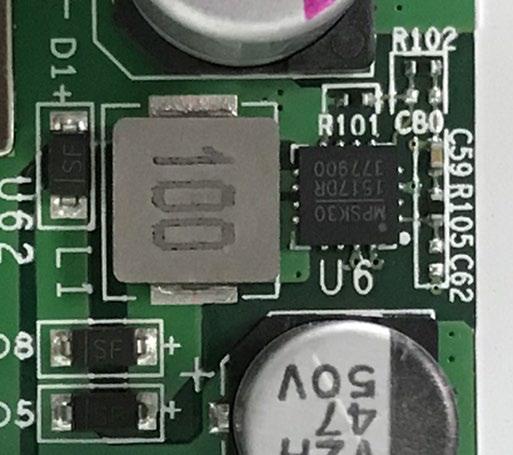
Figure 4-2
3. S17 chip signal direction:
3.1 CLK (XIN) signal direction: It is generated by Y1 25M crystal oscillator and transmitted from chip 01 to chip 65. During operation, the voltage is 1.45-1.65V(oscilloscope). Voltage measured by multimeter is about 0.7-0.9V.
3.2 TX (CI, CO) signal direction: input from pin 7 (3.3V) of IO port, transferred to IC U2 through level conversion, then transmitted from chip 01 to chip 65; the voltage is 0V when the IO line is not inserted, and the voltage during operation is 1.8V.
3.3 RX (RI, RO) signal direction: from chip 65 to chip 01, return to pin 8 of the signal cable terminal via U1 and return to the control board; the voltage is 0.3V when the IO line is not inserted, and the voltage during operation is 1.8V.
3.4 BO (BI, BO) signal direction: from chip 01 to chip 65; voltage measured using multimeter is 0V.
3.5 RST signal direction: input from pin 3 of the IO port, and then transmitted from chip 01 to chip 65; 0V without IO signal or in standby and 1.8V in operation.
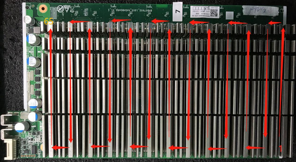
Figure 4-3
4. Overall architecture:
1. The machine is mainly composed of 3 hashboards, 1 control board, APW9 + power supply, and 4 cooling fans, as shown in Figure 4-4.
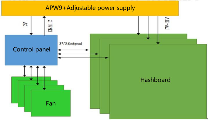
Figure 4-4
V. Common Poor Phenomenon of Hashboard and Troubleshooting Procedure
Phenomenon: during single board test, chip is detected to be 0 (PT1 / PT2 station type)
Step one: check the power output first. Please check the circled part in Figure 5-1.
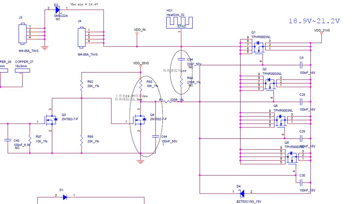
Figure 5-1
Step two: check the voltage domain voltage output
The voltage in each voltage domain is about 1.6V. Generally, there is a domain voltage when power is supplied at 21V. It is preferred to measure the output of the power supply terminal of the hashboard and determine whether the MOS is shorted (measure the resistance between pins 1, 4, and 8). If there is power supply at 21V but no domain voltage, continue to check downward.
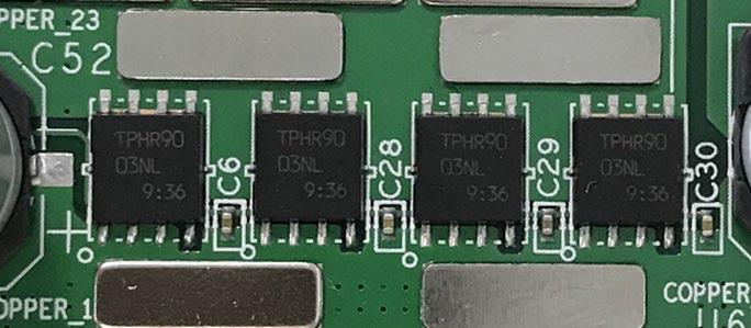
Figure 5-2
Step three: check the PIC circuit
Measure whether the second pin of U3 has an output, the voltage is about 3.2V; if yes, please continue to troubleshoot, if there is no 3.3V, please check that the connection status of the fixture cable and the hashboard is OK, and re-program the PIC.
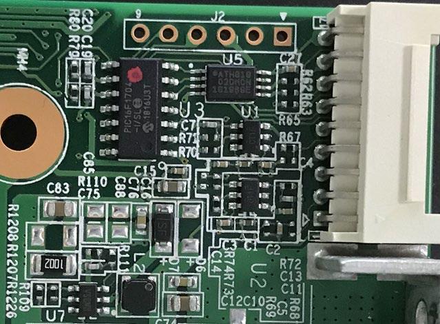
Figure 5-3

Figure 5-4
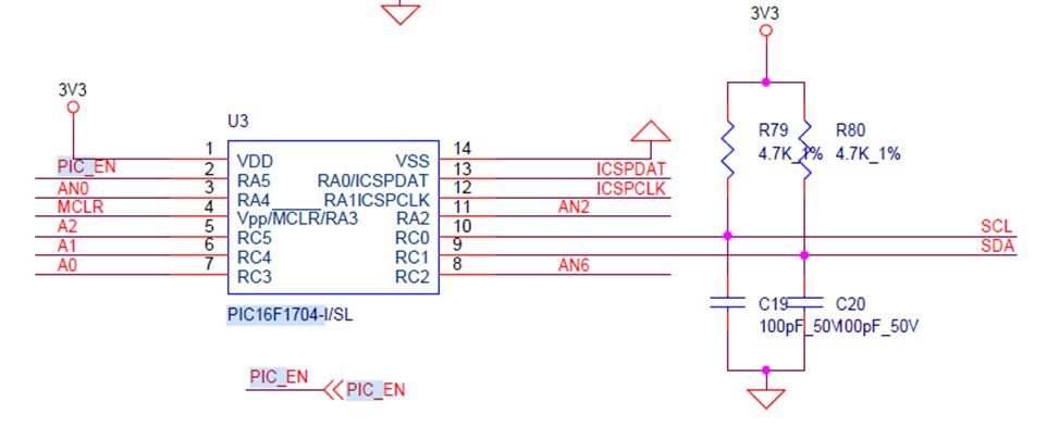
Figure 5-5
PIC programming procedure:
1. Program the PIC program of the arithmetic board.
Procedure: 20190908-PIC1704-BHB07602-0x88.hex
Download the programming tool: PICkit3; pin 1 of the PICkit3 cable corresponds to pin 1 of J3 on the PCB, and pins 1, 2, 3, 4, 5, and 6 need to be connected.
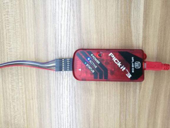
Figure 5-6
2. Programming software:
Open MPLAB IPE, select device: PIC16F1704, click power to select the power supply method, and then click operate. First step: select the file to find the .HEX file to be programmed. Second step: click connect to connect normally. Third step: click the program button, then click verify after finish. Prompt will be sent to prove that the programming is successful.
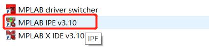
Figure 5-7
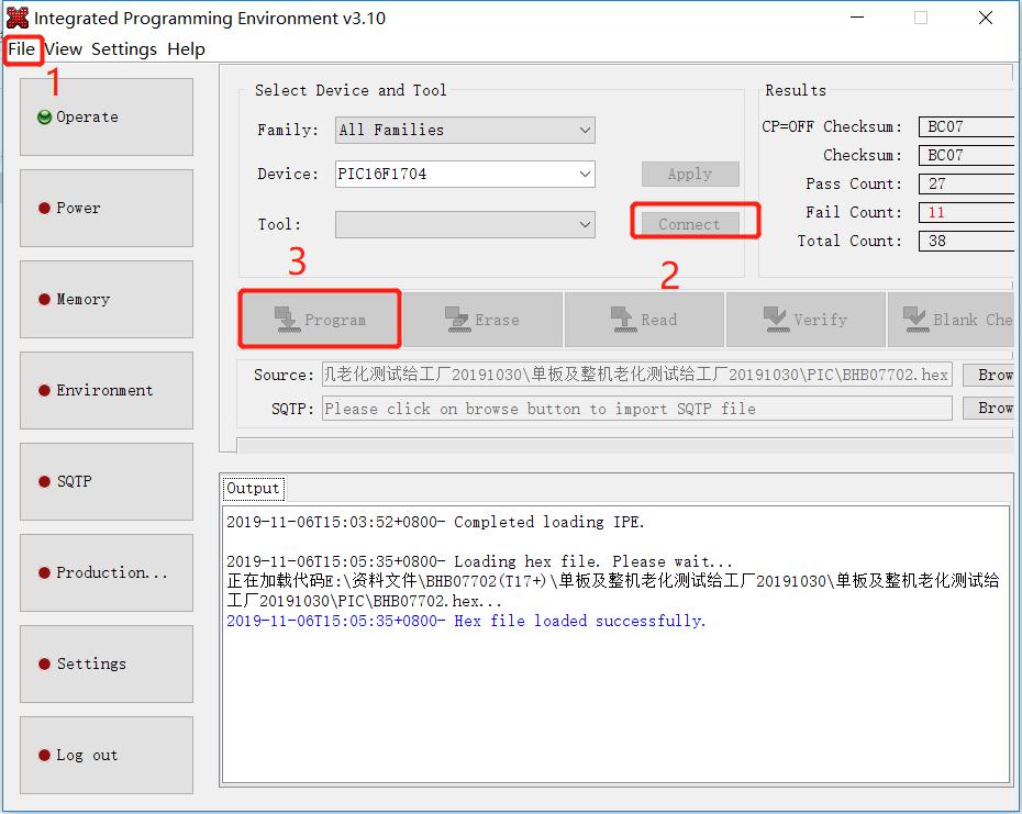

Figure 5-8
Step four: check the boost circuit output
Test D5 / D8 in chart 5-9 to measure 23-24.5V voltage.


Figure 5-9
Step five: check the LDO 1.8V or PLL 0.8V output of each group

Figure 5-10
Step six: check the chip signal output (CLK / CI / RI / BO / RST)
Refer to the range of voltage values described by the signal direction. If the measurement encounters a large deviation in voltage value, it can be compared with the measured values of adjacent groups.
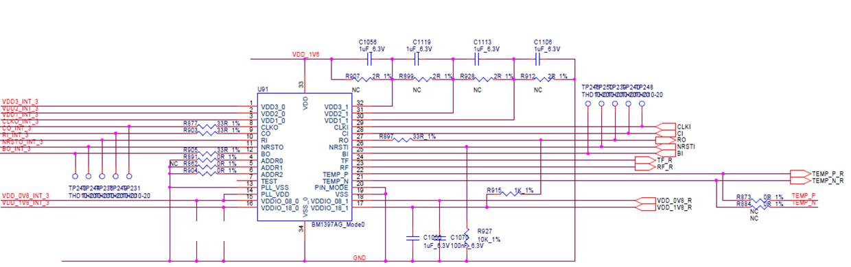
Figure 5-11
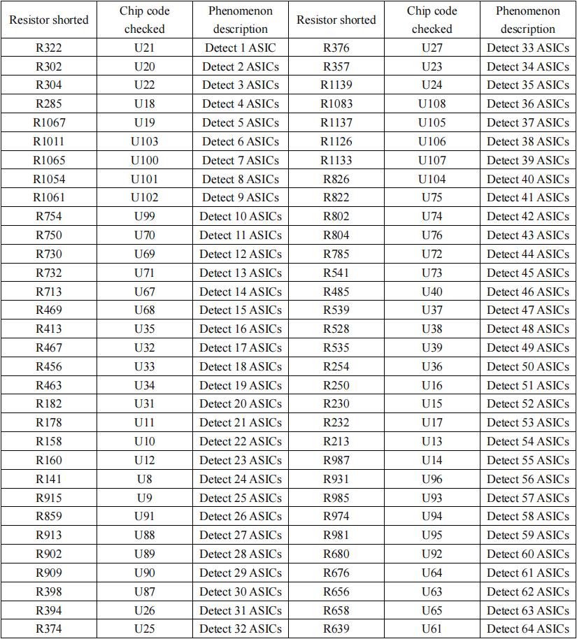
Assuming that the chip signal pin output voltage is normal, if the chip is still incomplete, for example, if 64 chips are detected, you can troubleshoot by shorting RO pull-up resistor R639. If 64 chips can be detected after shorting, it indicate that chips 1-64 should be normal, and you can troubleshoot the 65th chip at this time. If 63 chips are detected after short-circuiting, conduct troubleshooting forward; it is recommended to adopt the dichotomy method for troubleshooting, that is, test from the middle (starting from the 32th).

Figure 5-12
Troubleshooting comparison table:
Table 1
2. Phenomenon: Single board detection chip is incomplete (PT1 / PT2 station)
Check the relevant signals (CLK / CI / RI / BO / RST) of the chip in front of and behind the error position, locate the bad position according to the IC with the abnormal signal measured, and refer to the signal direction and voltage range for repair.
3. Phenomenon: single board pattern NG, that is, the response nonce data is incomplete (PT2 station type)
The serial port is connected to the computer, and the computer reads the test log; according to the results displayed in the log, the chip position of insufficient nonce data can be determined; replace the chip at the corresponding position.
4. Phenomenon: Test temperature reading is abnormal (PT2 station)
Check the temperature-sensing power supply VDD and the connection status between the temperature-sensing and the chip (TEMP_P; TEMP_N), and check the soldering quality of the chip connected to the corresponding temperature-sensing.
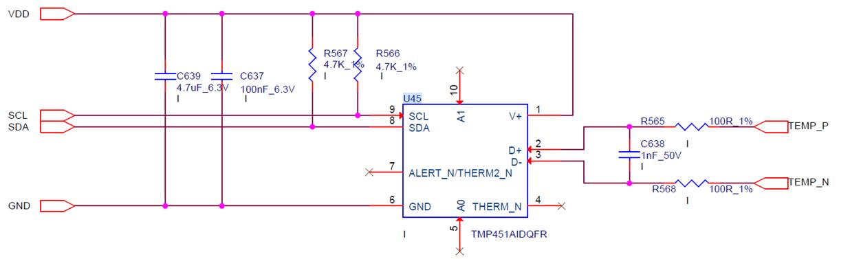
Figure 5-13

Figure 5-14
Check the quality of the front and back chip heat sinks connected to the temperature sensor. If the heat sink is not welded well, it will affect the temperature difference.
VI. Problems Caused by Control Board Issues
1. The whole machine is not running
First step: check whether the voltages at several voltage output points are normal. You can disconnect U8 first if 3.3V short circuit. If the short circuit still exists, you can unplug the CPU for measurement. For other voltage abnormalities, replace the corresponding transformer IC in general.
Second step: if the voltage is normal, please check the welding status of DDR / CPU (X-RAY inspection on the production side).
Third step: try to update the flash program with the SD card.

Figure 5-15
2.The whole machine cannot find the IP
Probably the IP is not found due to abnormal operation. Refer to point 1 for troubleshooting. Check the appearance and soldering of the network port, network transformer T1, and CPU.
3. The whole machine cannot be upgraded
Check the appearance and soldering of the network port, network transformer T1, and CPU.
4.The whole machine fails to read the hashboard or has fewer chains
A. Check the cable connection
B. Check the parts of corresponding chain on the control board
C. Check the wave soldering quality of the pins and the resistance around the plug-in interface
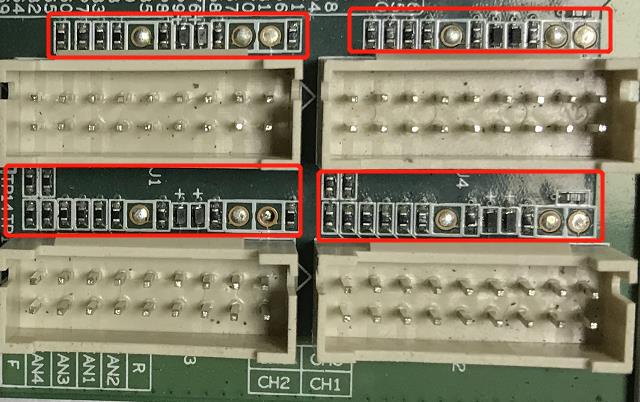
Figure 6-2
VII. Whole Miner Problems
1. Initial test of the whole machine
With reference to the test process documents, the general problems are assembly process issues and control board process issues.
Common phenomena: IP is not detected, the number of fans is abnormal, and the chain is abnormal.
2. The whole machine sweeping frequency band
Low hashrate caused by aging: Check the hashrate deviation of the corresponding hashboard to see if there is a large difference in hashrate, and take out the hashboard with a large hashrate deviation for test maintenance.
Check whether there's low average hashrate caused by the network interruption.
Large temperature difference caused by hashrate: check the aging environment; for the hashboard with high temperature, check the welding quality of the heat sink of the hashboard.
Aging machine protection: generally over-temperature protection is required, please control the aging environment temperature to be less than 40 degrees Celsius.
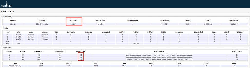
Figure 7-1
Less chain:
If one of the chains cannot be detected, disassemble the machine and test the corresponding hashboard; if it is determined that the hashboard is faulty, repair the hashboard; if it's determined that the control board is faulty, repair the control board.
Figure 7-2
4. After-sales maintenance
Refer to the above troubleshooting steps for each station. For related test procedures and hashboard testers, please communicate with the after-sales engineer for details. After repair, please use non-scanning mode to test PT2.
VIII. Other Matters Needing Attention
Maintenance flowchart
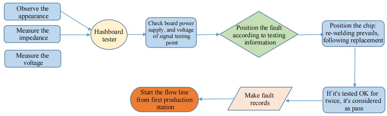
Figure 8-1 Maintenance flowchart
• Routine test: first perform visual inspection on the hashboard to be repaired, observe whether the PCB is deformed or burnt. If yes, it must be handled first; check whether there are any parts with obvious burn marks, collision offset or missing parts, etc.; secondly, if no problem is found through visual inspection, the impedance of each voltage domain can be tested first to detect whether there is a short circuit or an open circuit. If yes, it must be handled first. Third, check whether the voltage of each domain is about 1.5V.
• After the routine test is OK (in general, the short-circuit test is necessary for the routine test to prevent the chip or other materials from being burned due to short circuit when the power is on), you can use the hashboard tester to perform chip detection, and determine the positioning based on the hashboard tester test results.
• According to the display result of the test fixture test, test the voltages of chip test points (CO / NRST / RO / XIN / BI), VDD0V8 and VDD1V8, etc. starting from the vicinity of the faulty chip.
• According to the signal direction (the RX signal is passed in the reverse direction (from chip 65 to 1), and several signals CLK CO BO RST are transmitted in the forward direction (from chip 1 to 65), find the abnormal fault point through the power supply sequence.
• When locating to the faulty chip, the chip needs to be re-soldered. The method is to add a flux around the chip (preferably no-clean flux), and heat the solder joints of the chip pins to a dissolved status, so as to promote the chip pins and the pads to re-run, then removing tin finally, thus achieving the effect of re-tinning. If the failure is the same after re-soldering, the chip shall be replaced directly.
• The repaired hashboard can be determined to be a good product if it passes the fixture tests for more than twice. For the first time, after the replacement of the accessories is complete, wait for the hashboard to cool down and perform fixture test, after passing, set it aside and then cool it down; for the second time, wait for a few minutes until the hashboard is completely cooled before testing.
• After the board is repaired, relevant maintenance / analysis records (requirements for maintenance reports: date, SN, PCB version, tag number, bad cause, bad liability attribution, etc.) should be prepared for feedback to production, after-sales, research and development departments.
• After the record is prepared, install the entire machine for conventional aging.
• Good products repaired at the production end should flow production from the first station of production (at least conduct the appearance inspection and start from the PT1 / PT2 test station)!
Previous
Antminer S17 Hash Board Repair Manual
Read More
Next
Antminer/Whatsminer PSU Wake-up/Startup Tester Manual
Read More


