Antminer S17 Hash Board Repair Manual
By THANOS MINING
November 22nd, 2020
It mainly describes the troubleshooting of S17 various faults, and explains how to use the Antminer test fixture sold by ThanosMining for accurate positioning.
New version of test fixture: Antminer S17 test fixture
I. Service tools
1. General electric screwdriver
2. Multimeter, Tweezers, V9-v1.2 test fixture, S17 chassis with power supply
3. Heat gun (welding temperature is 260±2 degrees). Note: the temperature marked here is the actual temperature
4. Thermostat soldering iron (welding temperature is 300-350 degrees)
5. Environment-friendly scaling powder, lead-free low temperature (melting point 150 degrees) solder stick, anhydrous alcohol, water for cleaning panel;
6. OM550 low temperature solder paste, BM1397AE tin planting steel mesh fixture
7. Cooling fan;
II. Component structure of computing board
 III. Signal transmission circuit
1. Signal transmission channel, the signal CLK-RST-BO-CO is transmitted from the first chip to the second one, until the 48th; RI signal is transmitted from the 48th chip to the first chip reversely, as shown in following figure:
III. Signal transmission circuit
1. Signal transmission channel, the signal CLK-RST-BO-CO is transmitted from the first chip to the second one, until the 48th; RI signal is transmitted from the 48th chip to the first chip reversely, as shown in following figure:

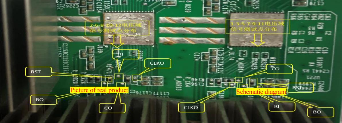
2. Signal test point identification and test point arrangement order (the computing board has a total of 48 chips, and 12 voltage domains) are as shown below:

Distribution of voltage domain test points

3. Signal communication circuit from IO block to chip
J1-IO block picture

Level switch IC

J1-IO block schematic diagram

 IV. Power circuit
1. The power supply voltage of each board (S17 fixture test voltage output is 18.5V). There are 12 voltage domains, and the voltage of every two voltage domains is 1.55v.
IV. Power circuit
1. The power supply voltage of each board (S17 fixture test voltage output is 18.5V). There are 12 voltage domains, and the voltage of every two voltage domains is 1.55v.

 V. Considerations for single board test
1. The computing board is not attached with cooling fin. The fixture program can only adopt the chip test program. After the chip is found, the cooling fin is attached.
V. Considerations for single board test
1. The computing board is not attached with cooling fin. The fixture program can only adopt the chip test program. After the chip is found, the cooling fin is attached.
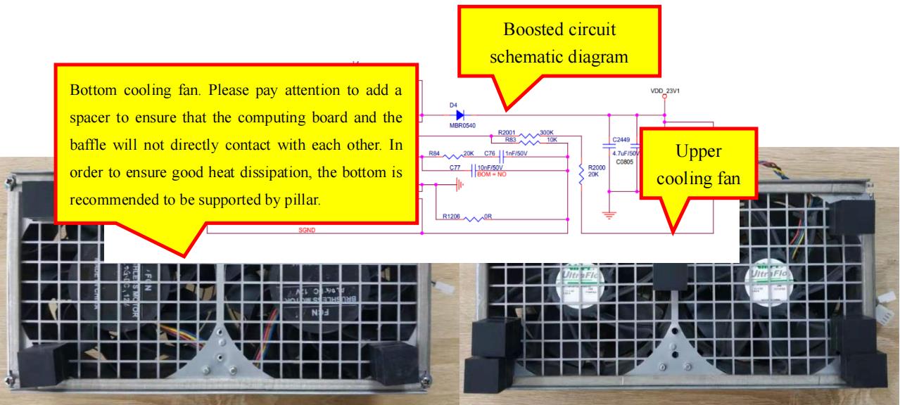
2. If the computing board needs to test parten, the heat dissipation requires 4 fans;
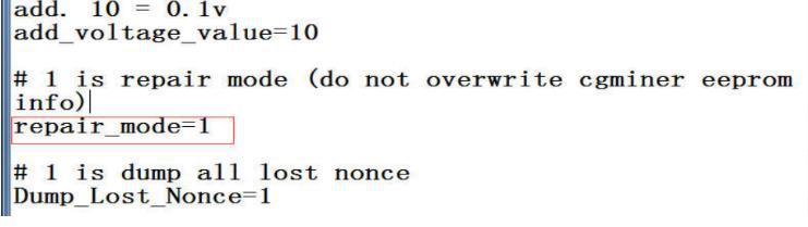
3. After sales, the machine in the condition of the software without sweeping frequency needs to change the repair mode under the fixture config file to 1, that is, the eeprom data is not cleared when testing;
 VI. Single board test troubleshooting example
6.1 single board fixture test asic=0
VI. Single board test troubleshooting example
6.1 single board fixture test asic=0
Failure analysis:
1. Whether the fixture cable and the computing board are in good contact.
2. If it's the S17 computing board, J6-J7 should have a voltage of 18.5V when testing the fixture.
3. When the fixture test is performing, whether there is a voltage between the 12 voltage domains, and the boost circuit is normal:
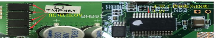
3.1 If there is no voltage in the voltage domain, it is necessary to check that the normal working voltage of the 4 pin of Q7Q8Q9Q11 is 0V. If it is high level, then check whether the 1 pin of Q10 is high level 3.3v. If Q10 does not have a voltage of 3.3v, it indicates that the U3-PIC loses firmware or is not powered.
PIC schematic diagram

18.5V output control circuit

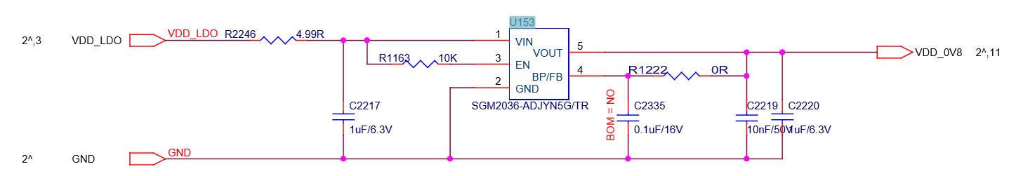
3.2 If the power supply is normal and the voltage of voltage domain is also available, then measure the RI signal of the chip to check if the RI signal has a voltage of 1.8V. When measuring the RI signal, it should be measured from the test point of the last chip, and if the last one has voltage, then measure the 20th chip for RI -1.8v. By analogy, when the chip has no RI output voltage is found, first measure it for the 1.8V power supply, if there is no power supply at 1.8V, then check the 1.8V power supply circuit. The 1.8V power supply circuit is obtained through voltage division by the voltage domain and then supply power to the LDO 1 pin. The LDO's 5 pin outputs 1.8V, (each voltage domain has one 1.8V LDO supplying power for the chip). If there is no output, there should be a problem with this LDO. If 1.8V is normal, measure the resistance value over the ground of the test point after power is cut off, and compare with the OK board to check if there is any resistance abnormality. If the value is normal and there is no problem in soldering, it should be that the chip has a fault, (weld the removed chip on a good board after planting tin, and then verity it. If there is no RI signal, it proves that the chip is damaged, so please replace the chip).

1.8V supply circuit

1.8V supply circuit
5.2 Fault phenomenon ASIC=7
Analysis: ASIC=7,
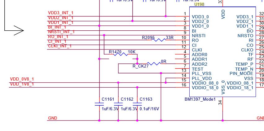
1. Single board test can find 7 chips, indicating that the RI signal is normal. The 8th chip cannot be found, so we shall directly measure the voltage of the 7th chip U198-CLK-RST-CO to check if the power supply is normal. If CLK does not have a voltage of 0.8V, then check the power supply circuit of CLK.
2-CLK circuit analysis: If CLK does not have 0.8V, first check whether the bad chip voltage domain 0.8V power supply is normal. The 0.8V power supply circuit is obtained by voltage domain divider and then supply power in the same way as 1.8V power supply mode. 5 pin output 0.8V maintenance method can refer to the 1.8V maintenance method (note that every two chips among the 4 chips of each domain of S17 can provide 0.8V LDO power supply, and every LDO supplies 2 chips)
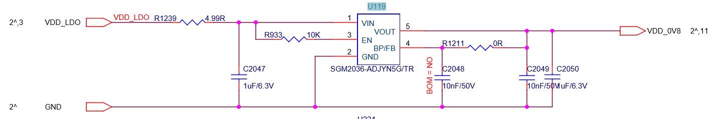
0.8v power supply scheme
If the 0.8V power supply circuit does not have a 0.8V output, then check if the 0.8V LDO power supply has a supply voltage of about 3.2V. If so, check whether the LDO is cold solder joint or short-circuited. If there is a 0.8V output, check the resistance of the chip over the ground. If the resistance is correct, it indicates the chip is damaged.
Previous
Antminer T17e Hash Board Repair Manual
Read More
Next
Antminer/Whatsminer PSU Wake-up/Startup Tester Manual
Read More


