Innosilicon T1/T2 Hash Board Repair Manual
By THANOSMINING
June 24th, 2020
Mainly describes how to troubleshoot various faults of the Innosilicon T1 T2 computing board, and explains how to use the test fixture sold by ThanosMining for accurate positioning.
New version of test fixture: Innosilicon test fixture
Scope: applicable to all T1 production, after‑sales, and outsourcing maintenance sites
1. Maintenance platform requirements:
Constant temperature soldering iron ( 350 Degree‑‑ 400 Degrees), the pointed soldering iron tip is used for soldering small patches such as chip resistors and capacitors.
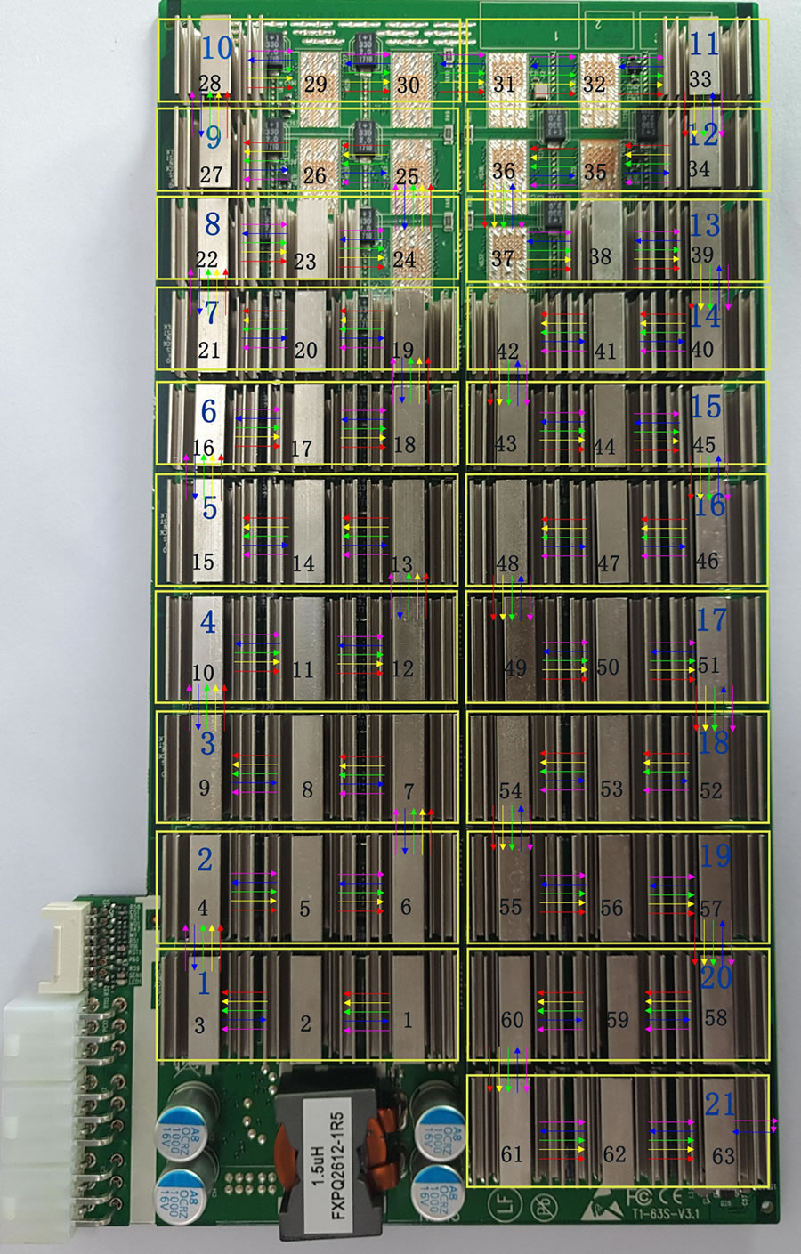
figure 1
Test whether the SPI waveform of the error‑reporting chip is normal; the picture above is the PCB board SPI Trend and voltage domain and chip sequence bit number
1. Each yellow box in the figure is a voltage domain, a total of twenty one Voltage domains, each voltage domain is on average 0.42V
2. The black numbers represent the order and bit number of the chip
3. The red arrow in the figure shows CLK Signal direction
The yellow arrow shows the direction of the SCK signal;
The green arrow shows the direction of the CS signal;
The blue arrow shows the direction of the DI signal;
The purple arrow shows the direction of the DO signal.
4. There is between every two chips 1‑7 Test point 1 for CLK Signal; test point 2 for RST Signal; test point 3 for EN Signal; test point 4 for SCK Signal; test point 5 for CS Signal; test point 6 for DI Signal; test point 7 for DO signal.
DI signal flow direction, from No. 63 chip to 1 Return the chip number, and then return to the control board;
DO signal flow direction, by 1 No. chip pulls low level toward 63; not plugged in IO Line, standby 0V , When calculating 0.3 Pulse signal around.
The RST signal flows in from the control board, and then by 1 Chip to 63 No. chip transmission.
2. The figure below shows the key circuits on the front of the T1 arithmetic board.
2 figure 2
1). Test points between each chip (as shown in the figure after zooming in): Figure 2
Figure 2. When repairing test points between chips, the test points between test chips are the most direct fault location
2) Voltage domain: The whole board has 21 voltage domains, and each voltage domain has 3 chips. The three chips in the same voltage domain are powered in parallel, and then connected in series with other voltage domains after being connected in parallel. The circuit structure is shown in Figure 4 below:
Principle analysis of voltage domain single chip (see Figure 3 below)
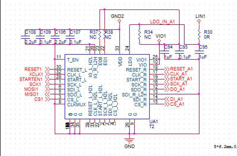
figure 3
● The above are the functions of each pin of the T1558 chip.
During maintenance, 14 test points before and after the chip are mainly tested (seven points before and after the chip: CLK , RST, EN , SCK, CS, DI, DO); DCDC Voltage output 8.82V;, boost voltage 11V, LDO‑‑1.8V, etc.
Detection method:
figure 4. The two ends of the C56 capacitor are the total DCDC output voltage, which should be about 8.82V
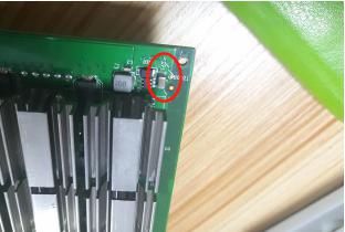
figure 5. Both ends of the C57 capacitor are the boost voltage, which should be about 11V
Figure 6. BM1558 circuit diagram
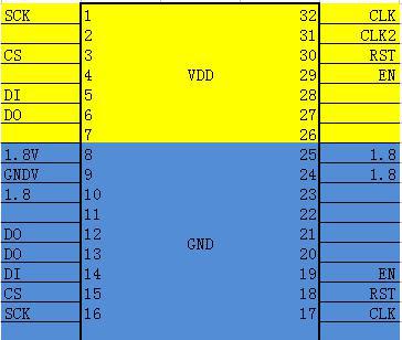
Figure 7. BM1760 chip pins
CLK: 0.9V provided by Y1 12M crystal oscillator
DO: From the first chip to the last chip provided by the control board, the signal can be measured with an oscilloscope
DI: Return from the last chip to the first chip, the signal can be measured with an oscilloscope
SCK: When the control board provides about 0.12V for calculation, the abnormal or low voltage will cause the calculation board to be abnormal or the calculation power is low
EN: 1.8V Provided by the control board
CS: Provided by the control board
RST: 1.8V . Provided by the control board, each time the test key is pressed, a low‑level reset signal will be output again.
When the above‑mentioned test point status and voltage are abnormal, please estimate the fault point based on the circuit before and after the test point.
It can be seen from the chart above:
CLK signal: by the chip 32 Or 31‑pin in, 17‑pin out, when connected across the voltage domain, by 5 Foot out through 100NF The capacitor is connected to the input to the next chip twenty three foot.
DO signal: enter from pin 6 of the chip, 12 Foot out
DI signal: returned by the chip from pin 5, output from pin 13 or 14;
CS signal: input from pin 3 of the chip and output from pin 15;
RST signal: by the chip 30 Foot in, 118 Pin output.
Test the signal voltage of each chip, LDO‑1.8OV
CORE: 0.8V‑‑‑ When this voltage is abnormal, it is usually the chip of the voltage domain CORE Short circuit
LDO‑1.8O: 1.8V‑‑‑‑ When this voltage is abnormal, the chip LDO‑1.8O Short circuit or open circuit
3) Judging the operating status of the computing board, the computing capability of the chip, and the temperature sensitivity based on the information in the printing window of the manufacturing tool.
3. O IO Definition
IO is composed of 2X7 pitch 2.0 PHSD 90 degree in‑line double row.

The pin definitions are shown in Figure 8 below:
As shown in FIG:
1 pin is LED
2 feet for VIDD
10.14 Feet: for GND .
3 feet are EN
4 feet for STAR
Pin 7 is PLUG
12 feet for SCK
13 feet are CS
8.9 Feet (DI, EO)
6 feet ( RST ): is the reset signal 3.3V Terminal, after being divided by resistors, it becomes 1.8V RST Reset signal.
5 feet ( 3V3 ): is the computing board 3.3V Power supply, the 3.3V Provided by the control board, mainly for PIC Provide working voltage.
TX_IN voltage is 1.8V
RST_IN voltage is 1.8V
4. Routine maintenance process:
● Reference steps:
1. Routine inspection: First, perform visual inspection on the arithmetic board to be repaired to observe whether there is any displacement, deformation, or scorching of the small heat sink? If any, you must deal with it first; if the small heat sink is displaced, remove it first, wash off the original glue, and re‑adhesive after the repair is passed.
Secondly, after the visual inspection is no problem, the impedance of each voltage domain can be tested first to detect whether there is a short circuit or an open circuit. If you find out, you must deal with it first.
Thirdly, check whether the voltage of each voltage domain reaches 0.42, and the voltage difference of each voltage domain shall not exceed 0.05V . The voltage of a certain voltage domain is too high or too low
Yes, the circuits in the adjacent voltage domains generally have abnormal phenomena. Need to investigate the reason first.
2. After the routine detection is no problem (generally, the short‑circuit detection of the routine detection is necessary, so as not to burn the chip or other materials due to the short circuit when the power is turned on), you can
Use DEBUG connection for chip detection, and judge and locate according to the detection result.
3. According to the display results of the test and detection, starting from the vicinity of the faulty chip, check the chip test points (CLK, RST, EN,
SCK, CS, DI, DO); DCDC voltage output 8.82V; boost voltage 11V, LDO‑‑ 1.8V etc.
4. Divide according to the signal flow direction DI Signal reverse transmission ( 6 To 1 Number chip), several of which signal CLK , RST , EN , SCK , CS ,, DO Is forward pass ( 1‑63 ), find the abnormal fault point through the power supply sequence.
5. When locating the faulty chip, the chip needs to be welded again. The method is to add flux around the chip (preferably no‑clean flux), and then insert the chip
When the solder joints of the pins are heated to a dissolved state, gently move up, down, left, and right to press the chip; the chip pins and the pads are re‑melted and the tin is collected. To achieve
The effect of tin is renewed. If the fault remains the same after re‑soldering, you can directly replace the chip.
6. The repaired computing board must be tested twice or more during testing. Two test times before and after: the first time, after the replacement of parts is completed, it is necessary
After the arithmetic board has cooled down and passed the test, put it aside first. For the second time, after a few minutes wait for the arithmetic board to cool down, test again. Although twice
The test time is a few minutes, but this does not affect the work. Put the repaired board aside, continue to repair the second board, wait for the second board to be repaired and placed
While cooling, test the first piece. In this way, the time is just staggered, and the total time is not delayed.
7. The repaired board. It is necessary to classify the faults and make records of the type, location, reason, etc. of the replacement components. For feedback back to production and after‑sales, Research and development.
8. After recording, install it into a complete machine for formal aging.
Five failure types:
1. The impedance of each voltage domain is unbalanced; when the impedance of some voltage domains deviates from the normal value, it indicates that there are parts in the abnormal voltage domain that have open circuits and short circuits. The most likely cause is the general chip. But there are three chips in each voltage domain, and often only one has a problem when it fails. Find out the problem chip
The method can detect and compare the test points of each chip to the ground impedance to find the abnormal point. If you encounter a short circuit, you can first use the same voltage on the chip.
Remove the hot plate first, and then observe whether the chip pins are connected to tin. If the short‑circuit point cannot be found in the appearance, you can find the short‑circuit point according to the resistance method or the current cut Waypoint.
2. Unbalanced voltage in the voltage domain;
When the voltage of some voltage domains is too high or too low, it is generally due to the abnormal voltage domain or the signal abnormality in the adjacent voltage domain, which leads to the following or down
A voltage domain works abnormally and the voltage is out of balance. Only by detecting the signal and voltage of each test point, the abnormal point can be found.
Compare the impedance of the test point to find out the abnormal point.
Observe the appearance, measure the impedance, measure the voltage, and detect the voltage and power supply of each test point. The test locates the chip according to the detection information, first re‑soldering, re‑soldering is invalid, replace it with the fault type record and test more than two times Ok can be considered as repaired Ok and then carry out related aging
Pay special attention to the fact that the CLK signal and RST Signal, these two abnormalities are most likely to cause voltage imbalance.
3. Lack of chip; Lack of chip means that the test box cannot detect all of them during testing. 63 For each chip, it is often impossible to detect as many chips as they actually are. However, the actual missing (undetected) abnormal chip is not in the displayed position. At this time, it is necessary to accurately locate the abnormal chip through testing.
The positioning method can use TX cut‑off to find the position of the abnormal chip. Is to convert a certain chip TX Signal to ground, for example: connect the first 50 Chip TX Output the ground of the voltage domain
After that, in theory, if all the previous chips are normal, 50 chips should be detected in the test box? If not detected 50 Chips, indicating that the abnormality is in the 50 Chip before; if 50 chips are detected, it means that the abnormal chip is after the 50th chip. By analogy, use dichotomy to find the location of the abnormal chip.
4. Broken link;
The broken link is similar to the lack of a chip, but the broken link does not mean that the chips that cannot be found are abnormal, but the abnormal chip behind the abnormal chip is caused by the abnormality of a certain chip.
All chips fail. For example, a chip itself can work, but it will not forward other chip information; at this time, the entire signal chain will suddenly stop here.
However, losing a large part of it is the broken link. Generally, the broken link can be displayed in the test box, for example: when the test box is testing the chip,
Only 14 chips are detected. If the preset number of chips is not detected in the test box, it will not run, so it will only display how many chips are detected.
At this time, just check the voltage and impedance of each test point before and after the 14th chip according to the displayed number "14" to find the problem.
5. Not running;
Not running means that the chip information of the arithmetic board cannot be detected in the test. E0:1 is the most common phenomenon, and the range of faults involved is wider.
1) Non‑operation caused by abnormal voltage in a certain voltage domain; the problem can be found by measuring the voltage of each voltage domain.
2) The abnormality caused by a certain chip abnormality can be found by measuring the signal of each test point.
CLK signal: the signal is generated by 1 No. chip output to 63 No. chip, but the current version has only two crystal oscillators, Y1(1‑30)X1(31‑63) of which as long as there is an abnormal signal clk Yes, all the following signals will be abnormal, search in order according to the signal transmission direction.
DO signal: This signal is caused by 1 , 2 , 3 ,,,,, 63 No. chip, when a certain point of the dichotomy is abnormal, it can be detected forward.
DI signal: This signal is caused by 63.60 , 59, 58, ,, 1 If the number returns, confirm the cause of the fault through the chip signal trend,
The signal is the highest priority if the T1 operation board is not running, and the signal is searched first.
RST signal: 1.8V ; After the arithmetic board is powered on and the 14P signal is plugged in, this signal will change from 01 , 02,, 0 63 The direction of the transmission to the last chip.
3) A certain chip VDD It can be caused by measuring whether the potential difference of each voltage domain is normal. Under normal circumstances, when the VDD voltage is 0.42, the normal voltage of each test point in other voltage domains is also 0.42 to ensure the balance between the voltage domains.
4) of a certain chip VDD1V8 Abnormal voltages Determine whether a certain VDD1V8 voltage is normal by measuring the test points of each voltage. Generally, the LDO voltage determines the voltage of each test point. When the LDO voltage is 1.8V, the normal voltage of each test point in other voltage domains is also 1.8. V
5. Low computing power;
Low computing power can be divided into:
1) During the test, received Nonce Insufficient, lack of computing power and show bad phenomena. This phenomenon can be judged by seeing the number of nonce returned by each
chip directly through the serial port printing information. Generally, the chip with the returned nonce number lower than the set value should be trouble‑shooted, and the non‑welding and external causes can be directly replaced. .
2) During the test of the test box, the computing power is low after the whole machine is installed. Most of this situation is related to the heat dissipation conditions of the chip, so special attention is required
The small heat sink of each chip is glued, and the ventilation performance of the whole machine. Another reason is that the voltage of a certain chip is critical. After the whole device is installed, the 12V power supply and
The difference in the power supply during the test leads to a deviation between the test hashrate and the running hashrate. You can use the test box to test after turning it down, and adjust the voltage slightly. DC adjustable power supply
After the 12V output, the chip is tested again to find the voltage domain with the lowest number of returned nonces.
6. A certain chip NG ;
Refers to when the test is passed, the test serial port information shows that the returned nonce of a certain chip is insufficient or zero. In addition to eliminating the problem of false soldering and peripheral components, you can
Replace the chip directly.
● Maintenance instructions:
1. During maintenance, the maintenance personnel must be familiar with the function and flow direction of each test point, the normal voltage value and the ground impedance value.
2. Must be familiar with chip soldering, so as not to cause PCB Foaming deformation or damaged pins.
3. T1558 chip package, both sides of the chip 16 foot. The polarity and coordinates must be aligned during welding, and they must not be misaligned.
4. When replacing the chip, the thermal conductive adhesive around the chip must be cleaned to avoid IC Hanging or poor heat dissipation during soldering may cause secondary damage to the chip.
Previous
Antminer S9k/S9se Hash Board Repair Manual
Read More
Next
Antminer/Whatsminer PSU Wake-up/Startup Tester Manual
Read More


