Bitmain APW8 Power Supply Repair Manual
By THANOS MINING
August 11th, 2020
It mainly describes the troubleshooting of various faults of the power supply APW8, and how to use the test tool for accurate positioning.
I. Requirements on the Maintenance Platform
1. The constant temperature soldering iron above 80W (soldering temperature: 300-350°C). The tip soldering iron head is used for soldering chip resistors and capacitors. The blade type soldering iron head is used for soldering and replacement of plug-in components (soldering temperature: 380-420°C)
2. The thermal chimney is used for chip disassembly and soldering, be careful not to heat for a long time to avoid PCB foaming (soldering temperature: 260°C ±2 °C).
3. The AC controllable power supply voltage regulator (output 200-250V, can limit 0-20A current) is used for APW8 power-on inspection. If there is no such condition, a 100W ordinary light bulb can also be strung on the AC fire line with mains. Be careful.
4. For electronic load (power 2KW, meet the voltage 0-50V), if there is no such condition, a resistive load that matches the APW8 can also be made.
5. The multimeter, suction gun, tweezers, V9-1.2 test jig and special power test card firmware (if there is condition, an oscilloscope can be configured).
6. Flux, lead-free tin wire, water for cleaning panel with anhydrous alcohol; water for cleaning panel is used to clean flux residue and appearance after maintenance.
7. Thermally conductive silicone grease (2500) is used to repair the thermal conduction between the MOS and the cooling fin, thermal conductive silicone (704 silica gel) is used for fixing and covering the glue damage at the original after the repair of the PCBA components
II. Requirements on Maintenance Operations
1. The maintenance personnel must have certain electronic knowledge, more than one year of maintenance experience, and a certain understanding of the working principle of switching power supply, and well master the soldering technology.
2. Before the product is opened and the PCBA panel is repaired, the large capacitor must be discharged, and the voltage must be measured with a multimeter (less than 5V discharge), and then the soldering operation can be performed! Be sure to confirm to avoid electric shock.
3. Pay attention to the working method when judging the circuit components. After replacing any device, the PCB panel has no obvious deformation, the soldering of bonding pad is reliable, and the replacement parts and the surrounding area have no problem such as insufficient parts, open circuit or short circuit.
4. After replacing the key components, the main circuit shall have no short circuit and other obvious abnormalities before the AC voltage test, otherwise there is a hidden danger of explosion.
5. It needs AC220V voltage to judge the circuit signal; pay attention to operational protection.
The following: Notes, key slogans
● Maintenance personnel qualifications must meet the specified requirements;
● Instruments and equipment used for maintenance must meet the specified requirements;
● The instruments and equipment for maintenance must be effectively grounded, and the maintenance environment must comply with anti-static requirements;
● Materials used for maintenance must meet the specified requirements; in order to guarantee the accuracy and traceability of the materials used for maintenance, the materials used for maintenance must be the production materials for the corresponding models, and the material replacement must be confirmed;
1. In order to prevent possible electric shock hazard, non-professionals should not disassemble the enclosure:
2. The maintenance personnel shall use a special enclosure opener to open the enclosure of power adapter and repair, to avoid damage to the internal components of the product:
3. After the product is opened, it is required to discharge the high voltage capacitor;
4. E-waste waste generated during product maintenance cannot be arbitrarily dropped:
5. Bad products must have a repair process card and indicate the cause of the failure, and placed separately;
6. The repaired products must be well marked to distinguish.
7. The repaired products must be placed in the repaired area and shall be systematically tested before they can be stored.
III. The Principle and Structure of the Power Supply
1. Principle overview
1.1 APW8 consists of 1 large panel, 2 fans and the upper and lower enclosures. The normal input AC220V has two DC output voltages, which are SB 12V respectively. The main voltage output is controlled by the PIC port and the mining machine communication, and different models’ DC voltage range is (8V-9.2V, 10V-11V, 16.32V-20.04V)
1.2 Performance characteristics and scope of use: S15, T15 with APW8 power supply 16.32V-20.04V as follows:
APW8 power supply is a high-efficiency DC power supply designed and manufactured by our company. It has single-phase AC input and two DC outputs:
1>. 16.32V-20.04V voltage adjustable output, the maximum current can reach 95A;
2>. 12V voltage fixed output, the current can reach 5A.
The adjustable output part of voltage can meet the common DC load use within 95A current of the adjustable voltage range, especially suitable for circumstances with strict requirements for power supply of servers and mining machines; the 12V voltage’s fixed output part can meet the use of control panel and cooling fin.
1.21 The are following characteristics:
●200-240V voltage input
●There is protection for undervoltage, short circuit, overload, over temperature, with automatic recovery after fault removal
●The use of high-quality devices ensures stable and reliable products through reasonable design, and can work at full load for a long time in a high temperature environment at 60°C or lower.
●Small size, high power density
1.3 Appearance of APW8 Power Supply
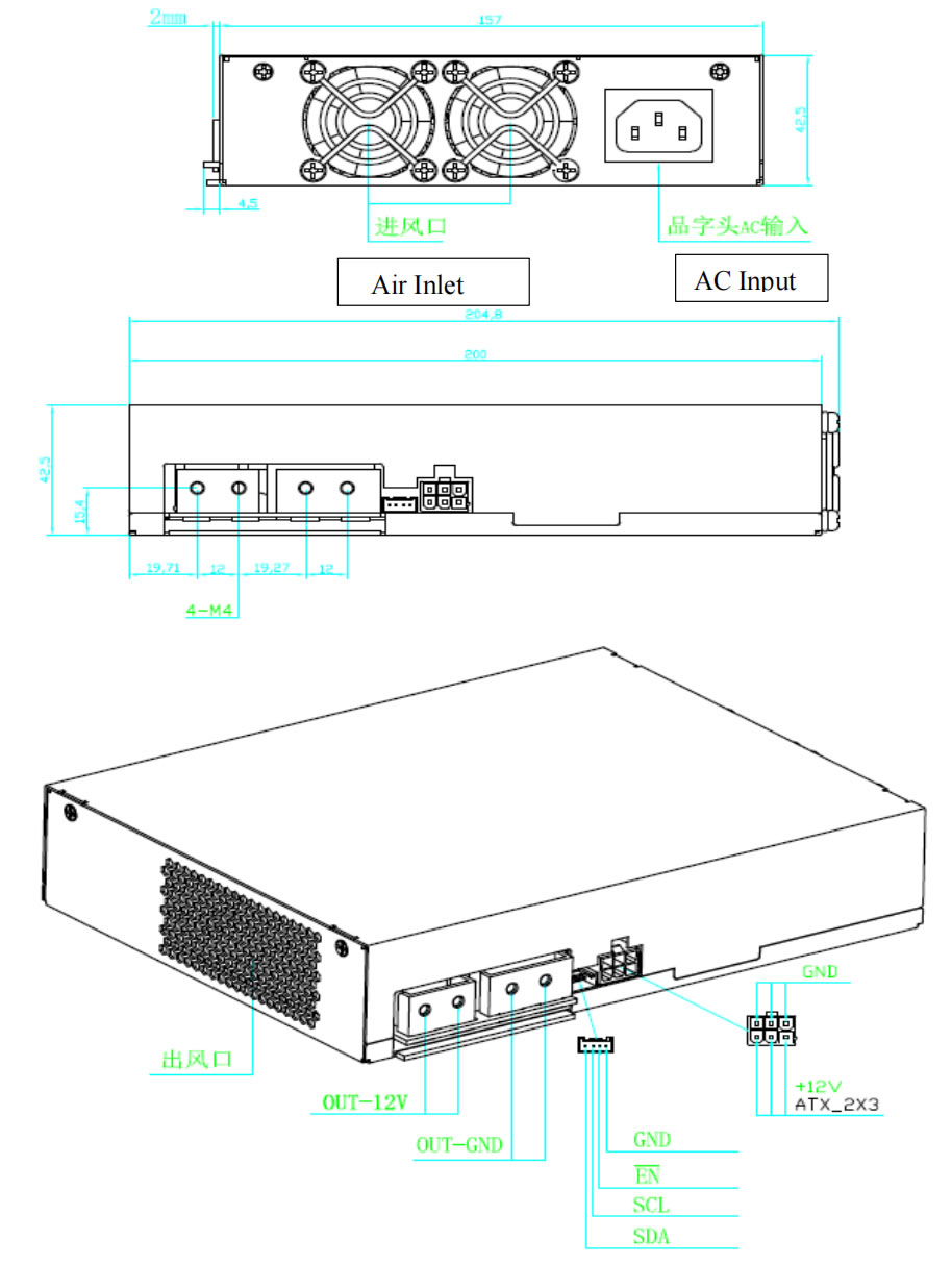
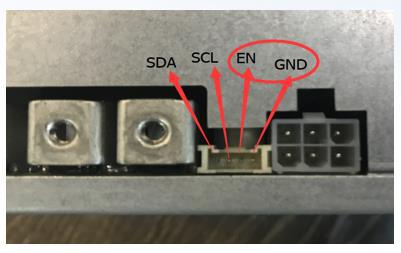
Note: If you need to turn on the default voltage 16.32V test, you can use the adapter cable to short connect the voltage Pin EN to GND.
● Distribution on the front panel of the power supply: one triangle-shape AC input interface
two size-4028 high speed fans
● Distribution on the left side of the power supply: four PCB-33 copper soldering terminals with adjustable voltage output
one 4Pin signal terminal
one 12V fixed voltage output PCIE terminal
● Distribution on the rear panel of the power supply: 1 set of air outlets, forming the air outlet of the high-speed fan.
● The model of the AC input terminal on the power supply front panel is C14, and the AC input cable of the C13 interface is required.
● The 4Pin signal terminal is the interface between the external control panel and the power supply. The SDA/SCL is the I2C protocol, and can adjust the output voltage of the power supply through I2C. EN is the enable signal of the power supply, and the control panel can enable the power supply through EN, which is effective in low level.
● The output part of the adjustable voltage adopts four PCB-33 copper soldering terminals, 90-degree side foot binding posts, M4 high current horizontal fixed seat; the 2 terminals close to the air outlet are output positive poles, and 2 near signal terminals are output negative poles, the output line or output copper bar can be fixed on terminal by M4 screw, which is convenient and flexible to use.
● The output part of the 12V fixed voltage uses the PCIE output terminal. The PCIE output terminal diagram is as follows:

The PCIE output line consists of two color lines, the 12V positive line is yellow, and the negative s line is black.
Definition of 6PIN PCIE terminal positive and
negative poles:
Positive pole: yellow 1, yellow 2, yellow 3
Negative pole: black 4, black 5, black 6
1.4 Parameters of APW8 Power Supply:

2. Maintenance ideas and cases of common faults
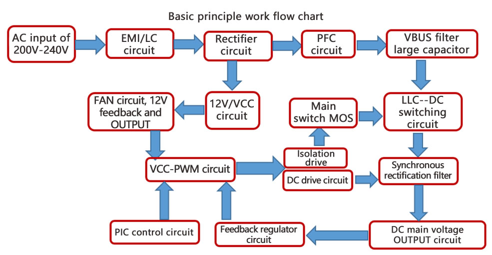
2.1 Block diagram for power basic principle
2.2 Power PCBA board layout
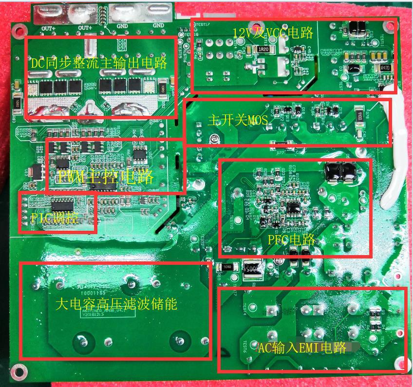
DC 同步整流主输出电路:Main output circuit of DC synchronous rectification
12V 及 VC 电路:12V and VC circuits
主开关 MOS:Main switch MOS
PWM 主控电路:PWM main control circuit
PIC 调控:PIC regulation
PFC 电路:PFC circuit
大电容高压滤波储能:Large-capacity high-voltage filter energy storage
AC 输入 EMI 电路:AC input to EMI circuit
Physical picture, there will be small differences in product versions, but the principle is similar.
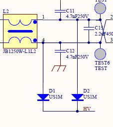
2.21 AC inputs EMI to PFC circuit schematic, focus on measuring whether F1 insurance, U2 rectifier bridge, Q4, D7, D5, D6 are damaged.
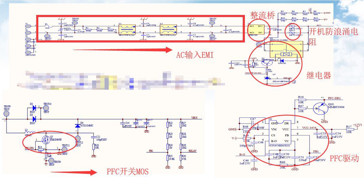
整流桥:Rectifier bridge
AC 输入 EMI:AC input to EMI
开关防浪涌电阻:Switch anti-surge resistor
继电器:Relay
PFC 开关 MOS:PFC switch MOS
PFC 驱动:PFC driver
2.22 12V auxiliary circuit principle, focus on measuring whether voltage detection starts resistor R33, 47K and connecting with HV to D1, D2, and whether Q5, D8, D9, T1 is damaged.
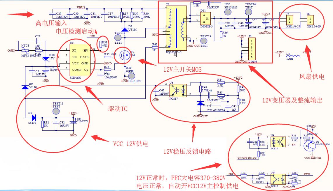
高电压输入:High voltage input
电压检测启动:Voltage detection starts
12V 主开关 MOS:12V main switch MOS
驱动 IC:Driver IC
VCC 12V 供电:VCC 12V power supply
风扇供电:Fan power supply
12V 变压器及整流输出:12V transformer and rectifier output
12V 稳压反馈电路:12V regulated feedback circuit
12V 正常时,PFC 大电容 370-380V 电压正常,自动开 VCC12V 主控制供电:When 12V is normal, the PFC large capacitor 370-380V voltage is normal, and the VCC12V main control power supply is automatically turned on
2.23 The main control PWM drive circuit, PIC control voltage regulation schematic diagram, focus on the main IC VCC power supply and drive transformer.
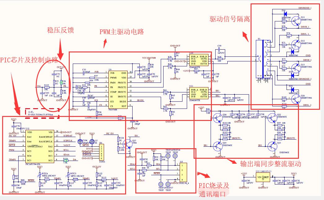
稳压反馈:Voltage regulation feedback
PWM 主驱动电路: PWM main drive circuit
PIC 芯片及控制电路: PIC chip and control circuit
PIC 烧录及通讯端口: PIC burning and communication port
输出端同步整流驱动: Synchronous rectification drive at output end
驱动信号隔离: Drive signal isolation
2.24 Main switch MOS and transformer conversion buck synchronous rectification DC filter output circuit, focus on the main switch MOS Q14; Q15; Q6; Q16, the output rectifier side positive and negative have no short circuit.
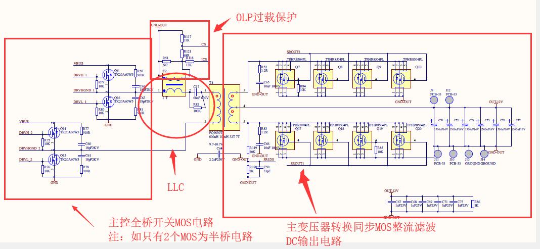
OLP 过载保护:OLP overload protection
主控全桥开关 MOS 电路:Master control full bridge switching MOS circuit
注:如只有 2 个 MOS 为半桥电路:Note: If there is only 2 MOS, it is a half-bridge circuit
主变压器转换同步 MOS 整 流 滤 波 :Main transformer conversion synchronous MOS rectification filter
DC 输出电路: DC output circuit
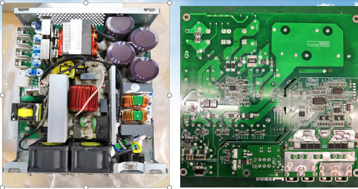
2.25 Location of A side of SMD patch and B side of plug-in

Figure 1 SMD patch side location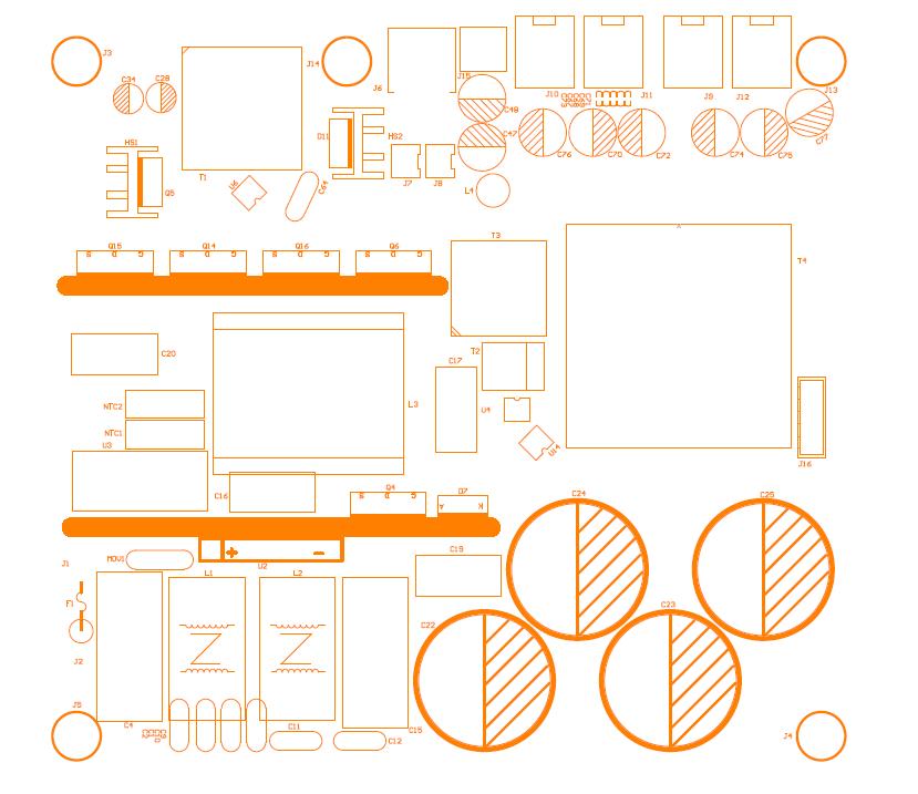
Figure 2 Plug-in side location
2.31. Check whether the appearance of the power supply is seriously damaged or deformed, and whether the DC fan and the AC socket are damaged.
2.32. Power on AC220V, check whether the fan is rotating normally, and use the multimeter to measure whether the output J6 terminal’s voltage is 12V (12.1V-12.50) to eliminate measuring error
2.33. Open the enclosure to check whether the components and solder surface have sparking phenomenon (focus on whether the R33 resistor is damaged), use a multimeter to detect whether the AC input terminal’s F1 fuse has open circuit, whether the U2 rectifier bridge; PFC MOS Q1; D7; D5; D6 have short circuit, whether the PWM circuit’s main switches MOS Q6; Q14; Q15; Q16 and output patches MOS Q17; Q18; Q19; Q20 have short circuit; if there is a short circuit, the component position should be checked and replaced, pay attention to the circuit resistance around bad bit MOS tube; the transistor may be damaged and needs to be replaced.
2.34. Detect whether the auxiliary 12V circuits U5; T1; Q5; D11 have short circuit or open circuit, and whether the surrounding components are burned, etc., replace if necessary.
2.35. If there is no abnormality in the above locations, the F1 fuse path is normal. After the AC is powered on, the DC fan rotates (if there is no rotation, check whether the fan socket has voltage of 12V, if the voltage is normal, replace the fan); the output terminal J6 has 12V voltage, measure whether there is DC370V-380V at both ends of PFC large capacitor C16 or C17, otherwise check whether U1, pin 7V VCC power supply has 12V or judge material damage and replace, if there is no abnormality, it needs to detect PWM circuit U9; U10; U11; whether supply VCC has 12V voltage or judge material damage and replace, and whether the T4 drive transformer is damaged.
2.36. other bad needs to be further analyzed and judged according to the skills of maintenance personnel, After the above check, the single power supply test main circuit DC output needs to be short connected to the J15 PIN 4-5, as EN-GND pin shown in the figure. Note that short connection errors may damage the chip. After the defective device is replaced and the soldering is correct, the AC220V test can be performed.
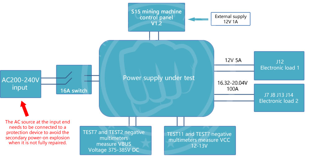
2.4 Diagram for electrical function test connection, PCBA main voltage measurement point.
(1) Test equipment: power meter, multimeter, electronic load, or other similar automatic test equipment. (When the DC output is normal, it can be tested with a mining machine if there is no load).
(2) The test connection diagram is as follows:
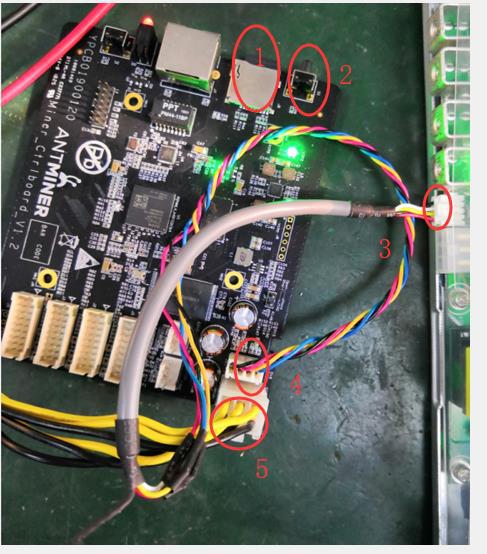
2.41 Diagram for S15 control panel V1.2 and APW8 power PIC port connection test, label 1 is the dedicated card test firmware, 2 is the DC voltage debugging high-low conversion button, 3 is the PIC communication port, 4 is the control panel socket, 5 is 12V power supply; note that yellow indicates positive and black indicates negative. Note: After the general power supply defective products are repaired, the power supply only needs to be short connected with the PIC communication J15 port EN-GND pin, and if there is voltage output 16V, it is normal, and the following single test for the control panel is not requried (when the PIC single chip is damaged, or when the firmware is abnormal, it needs to test a small panel before re-burning), and the corresponding mining machine test can be directly installed.
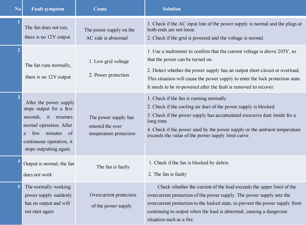
2.5 Simple judgment and maintenance of common faults of mine power supply
2.6 After the power supply maintenance test is normal, it is required to operate normally for 2 hours with the rated load of 80% (80A) or more before it can be used by the client.
Previous
WhatsMiner M20S Hash Board Repair Manual
Read More
Next
Antminer/Whatsminer PSU Wake-up/Startup Tester Manual
Read More


