Antminer T17 Hash Board Repair Manual
By THANOS MINING
October 18th, 2020
It mainly describes the troubleshooting of various faults of T17, and explains how to use the Antminer test fixture sold by ThanosMining for accurate positioning.
New version of test fixture: Antminer T17 test fixture
I. Maintenance Tools
1. General electric screwdriver
2. Multimeter, tweezers, V9-v1.2 test jig, S17 chassis with power set
3. Hot air gun (welding temperature is 260 degrees±2 degrees)
4. Constant temperature soldering iron (welding temperature is 300-350 degrees)
5. Environmentally friendly flux, lead-free low temperature (melting point at 150 degrees) solder wire, anhydrous alcohol, water for cleaning panel,
6. OM550 low temperature solder paste, BM1397AE tinning steel mesh jig
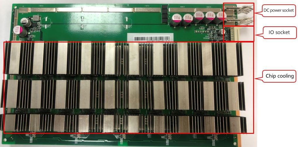
II. Component Structure of the Hash Board
 III. Signal Transmission Circuit
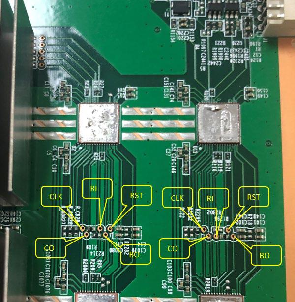
1. Signal transmission channel, signal CLK-RST-BO-CO is transmitted from the first chip to the second, and till the 72nd, RI signal is reversely transmitted from the 72ndchips to the first chip, as the figure below:
III. Signal Transmission Circuit
1. Signal transmission channel, signal CLK-RST-BO-CO is transmitted from the first chip to the second, and till the 72nd, RI signal is reversely transmitted from the 72ndchips to the first chip, as the figure below:

2. Signal test point identification and test point arrangement order (there are a total of 48 chips on the hash board, and 12 voltage domains), as shown below:

Distribution of test points in voltage domain


3. Signal communication circuit from IO socket to chip
Picture of J1-IO socket


Schematic diagram of J1-IO socket

 IV. Power Circuit
1. The power supply voltage of each board is (T17 jig test voltage output is 17V). There are 10 voltage domains, and the voltage of each two voltage domains is 1.7V.
IV. Power Circuit
1. The power supply voltage of each board is (T17 jig test voltage output is 17V). There are 10 voltage domains, and the voltage of each two voltage domains is 1.7V.
V. Cases of Single Board Test Troubleshooting
5.1 Single board jig test asic=0
Failure analysis:
1. Whether the jig cable and hash board are in good contact.
2. The T17 hash board J6-J7 should have a voltage of 17V when testing the jig
3. When testing the jig, measure whether there is voltage between the 10 voltage domains.
3.1 If there is no voltage in the voltage domain, it is necessary to see whether the normal working voltage of the pin 4 of Q7Q8Q9Q11 is low level of 0V. If it is high level, then it depends on whether the pin 1 of Q10 is high level of 3.3v, if Q10 does not have 3.3V Voltage, that is, U3-PIC loses firmware or there is no power supply

Schematic diagram of PIC

17V output control circuit

3.2. If the power supply is normal and there is voltage in voltage domain, then the RI signal of the chip should be measured to see if the RI signal has a voltage of 1.8V. When measuring the RI signal, it should start from the test point of the last chip. If there is voltage in the last chip, measure whether the 20th chip has RI -1.8v, and the rest can be done in the same manner, when finding the chip that does not have RI output voltage, first measure the 1.8V power supply of this chip, if there is no power supply of 1.8V, then check the 1.8V power supply circuit. The 1.8V power supply circuit is supply powers to the LDO pin 1 through the voltage division of the voltage domain. The pin 5 of LDO outputs voltage of 1.8V. (Each voltage domain has -1.8 V LDO to supply power to chip). If there is no output, this LDO should have a problem. If 1.8V is normal, measure the ground resistance of the test point after the power is cut off and compare with the OK board to see if there is any resistance abnormality; if the resistance value is normal, and there is no problem with soldering. This chip should have a problem. (Re-tin the removed chip and solder it to a good board to verify it. If there is no RI signal, it proves that the chip is damaged, replace the chip. )
1.8V power supply circuit


5.2 Fault phenomenon is ASIC=7
Analysis: ASIC=7,
1. In a single board test, 7 chips can be found. It can be judged that the RI signal is normal. If the 8th chip cannot be found, we will directly measure the voltage of the 7th chip U198-CLK-RST-CO to see if the power supply is normal. If CLK does not have a voltage of 0.8V, then it depends on the power supply circuit of CLK.
2. CLK circuit analysis: If CLK does not have 0.8V, first check whether the 0.8V power supply of the bad chip voltage domain is normal, the 0.8V power supply circuit is obtained by voltage domain division, and 1.8V power supply mode is the same, as for the maintenance method for pin 5 output 0.8V, refer to the 1.8V maintenance method (note that there are 2 out of 3 chips outputting 0.8V LDO power supply in each chip in each domain of T17, and each LDO supplies to 2 chips)
0.8v power supply schematic


If the 0.8V power supply circuit does not have a 0.8V output, then see if the 0.8V LDO power supply has a supply voltage of about 3.2V. If it has, see if the LDO is soldered insufficiently or short-circuited. If there is a 0.8V output, then see the ground resistance of the chip, if the resistance is correct, it should be a bad chip.
Previous
Antminer S15 Hash Board Repair Manual
Read More
Next
Antminer/Whatsminer PSU Wake-up/Startup Tester Manual
Read More


